
Page 370 - System on Package_ Miniaturization of the Entire System
P. 370
342 Cha pte r S i x
Laser
driver
Digital in
I
Decision
TIA circuit Digital out
L/A Filter
Light in
Clock
Auto gain recovery
control
Front end Signal conditioning Data recovery
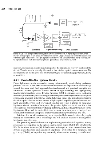
FIGURE 6.12 Key components employed in optical interconnects. A digital signal is converted
into an analog signal by the direct modulation of current I. Light pulses are emitted in accordance
with the digital modulation. The light signal is introduced into and transmitted along a waveguide
to a photodetector that absorbs the light and generates a proportional current.
recovery, and decision circuits may form part of the digital data recovery portion of the
circuit. The circuitry is virtually identical to that of data optical communications. The
requirements on the bit error rate are more stringent for computing applications, being
–15
at least 10 .
6.6.1 Passive Thin-Film Lightwave Circuits
Planar lightwave circuits are used to convey information by manipulating packets of
photons. The idea is similar to electric circuits that make use of packets of electric charge
toward the same end. Each approach has fundamental and practical strengths and
limitations. Planar lightwave circuits consist of light-confining and light-guiding
functions (waveguides), power dividing functions (MMI, Y-splitters), power combining
functions (Y-combiners), and wavelength combining and spreading functions (waveguide
phase array gratings). Ultimately, a useful lightwave circuit also includes interfaces to
electrical-optical devices such as sources of light; optical amplifiers; photodetectors; and
light amplitude, phase, and wavelength modulators. Thus a planar or nonplanar
lightwave circuit consists of two parts, the passive lightwave circuit and the active
optoelectronic components for producing, detecting, and encoding information on the
light carrier. How well the optical interface between these two parts is designed and
constructed determines the optical interconnect reliability, performance, and cost.
In this section we will consider only some aspects of lightwave circuits as they apply
directly to optoelectronic SOP technology and will indicate sources of more general
treatments along the way.
The prevailing state-of-the-art for implementing optical-digital signaling among
processors is exemplified by the optical electric circuit board (OECB) [51] of which the
IBM Terabus is an extension [55]. In both cases, active optical components—lasers, laser
drivers, photodetectors, and associated amplifiers—are bonded to a peripheral ball
grid array (PBGA) package that may eventually also contain a memory controller with