
Page 369 - System on Package_ Miniaturization of the Entire System
P. 369
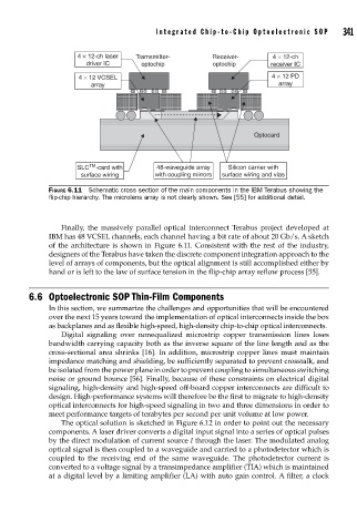
Integrated Chip-to-Chip Optoelectr onic SOP   341


                            4 × 12-ch laser  Tramsmitter-      Receiver-      4 × 12-ch
                              driver IC     optochip           optochip       receiver IC

                            4 × 12 VCSEL                                      4 × 12 PD
                               array                                            array


                                                                         Optocard


                            SLC TM -card with   48-waveguide array  Silicon carrier with
                             surface wiring     with coupling mirrors  surface wiring and vias

                    FIGURE 6.11  Schematic cross section of the main components in the IBM Terabus showing the
                    fl ip-chip hierarchy. The microlens array is not clearly shown. See [55] for additional detail.


                       Finally, the massively parallel optical interconnect Terabus project developed at
                    IBM has 48 VCSEL channels, each channel having a bit rate of about 20 Gb/s. A sketch
                    of the architecture is shown in Figure 6.11. Consistent with the rest of the industry,
                    designers of the Terabus have taken the discrete component integration approach to the
                    level of arrays of components, but the optical alignment is still accomplished either by
                    hand or is left to the law of surface tension in the flip-chip array reflow process [55].


               6.6 Optoelectronic SOP Thin-Film Components
                    In this section, we summarize the challenges and opportunities that will be encountered
                    over the next 15 years toward the implementation of optical interconnects inside the box
                    as backplanes and as flexible high-speed, high-density chip-to-chip optical interconnects.
                       Digital signaling over nonequalized microstrip copper transmission lines loses
                    bandwidth carrying capacity both as the inverse square of the line length and as the
                    cross-sectional area shrinks [16]. In addition, microstrip copper lines must maintain
                    impedance matching and shielding, be sufficiently separated to prevent crosstalk, and
                    be isolated from the power plane in order to prevent coupling to simultaneous switching
                    noise or ground bounce [56]. Finally, because of these constraints on electrical digital
                    signaling, high-density and high-speed off-board copper interconnects are difficult to
                    design. High-performance systems will therefore be the first to migrate to high-density
                    optical interconnects for high-speed signaling in two and three dimensions in order to
                    meet performance targets of terabytes per second per unit volume at low power.
                       The optical solution is sketched in Figure 6.12 in order to point out the necessary
                    components. A laser driver converts a digital input signal into a series of optical pulses
                    by the direct modulation of current source I through the laser. The modulated analog
                    optical signal is then coupled to a waveguide and carried to a photodetector which is
                    coupled to the receiving end of the same waveguide. The photodetector current is
                    converted to a voltage signal by a transimpedance amplifier (TIA) which is maintained
                    at a digital level by a limiting amplifier (LA) with auto gain control. A filter, a clock