
Page 368 - System on Package_ Miniaturization of the Entire System
P. 368
340 Cha pte r S i x
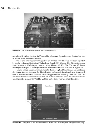
FIGURE 6.9 Top view of the ETHZ-IBM demonstrator board.
comply with pick-and-place SMT assembly tolerances. Optoelectronic devices have to
fit within these process tolerances.
End-to-end optoelectronic integration on printed circuit boards has been reported
by the Swiss Federal Institute of Technology, Zurich (ETHZ), and IBM Rüschlikon, over
o
four channels at 10 Gb/s per channel, using 850-nm VCSEL, PIN PDs, and 45 beam
turning mirrors [53]. A photograph of the demonstrator board is shown in Figure 6.9.
Flexible optical interconnects, similar to those of Optical CrossLinks, are just being
developed to meet the need for high-density, high-speed, interboard, and intraboard
optical interconnections. The latest paper to appear is that from Ray Chen, SCI [54]. The
o
resulting structure is shown in Figure 6.10. As in all previous cases, 45 end mirrors are
used here also along with VCSELs and top (or bottom) viewing photodetectors.
Micro mirrors
VCSEL array GaAs PIN array
1 × 12 waveguide array
FIGURE 6.10 Integrated VCSEL and PIN detector arrays on a fl exible optical waveguide fi lm. [54]