
Page 399 - Sami Franssila Introduction to Microfabrication
P. 399
378 Introduction to Microfabrication
Gas sensing area Electronic IC area
NMOS PMOS
Sensor
S D S D
SiO 2 SiO 2 SiO 2 SiO 2
n+ p n+ n+ p n+ p+ n p+
SiO 2 SiO 2
Heater
Si Silicon Sensitive layer Si Si
Oxide Metal n substrate
Polysilicon Passivation layer
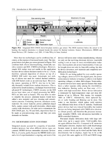
Figure 39.6 Integrated SOI–CMOS micro-hot-plate resistive gas sensor. The MOS transistor below the sensor is for
heating; the readout electronics is situated beside the sensor for thermal isolation. Source: Microsensors, MEMS and
Smart Devices, J.W. Gardner et al, 2001, John Wiley & Sons, Limited
More than two technologies can be combined, but, of devices will never enter volume manufacturing, whereas
course, at the expense of increased mask count. The inte- we only see the surviving electronic devices. Linewidth
grated micro-hot-plate gas sensor pictured in Figure 39.6 scaling is not an issue in most microfabrication indus-
combines bulk silicon micromachining, chemically sen- tries: microsystems aim at new functionalities. Costs can
sitive resistors and SOI–CMOS technologies. However, be brought down not only by linewidth scaling, but also
simple SOI wafers were not usable in this application by device cleverness, new materials and completely new
because device silicon thickness needs to be ca. 1.5 µm, fabrication technologies.
therefore, epitaxial deposition of silicon on top of a While ICs are being pushed for even smaller operat-
SIMOX SOI wafer was used. Anisotropic wet etch- ing voltages, down to 0.35 V for digital parts, the power
ing of silicon was used for vertical thermal isolation, semiconductor industry is hoping to achieve even higher
with SOI buried oxide as an etch-stop layer. However, operating voltages, or rather, kilovoltages. Semiconduc-
the sensor, operating at 350 C, also has to be later- tor power devices have many special features that make
◦
ally thermally isolated from readout electronics. This is them a rather separate entity among the microfabrica-
achieved by trench isolation, a technique borrowed from tion industries. Starting wafers are float zone <111>
advanced IC technologies. CMOS circuitry on the SOI wafers with high resistivities. Power device fabrication
device layer takes care of signal processing but MOS- is dominated by high-temperature steps and deep dif-
FETs are also used as heaters. This was done in order fusions of up to 100 µm. This means, for example,
to simplify the process: platinum heaters would have 100 h at 1200 C. Alternatively, thick epitaxial lay-
◦
added a new material, and new cleaning and contami- ers or wafer bonding and thinning can be done. One
nation concerns. Contacting, however, introduces exotic wafer is one thyristor, which makes yield statistics
materials: the sensor material, porous palladium-doped very different from those of the IC industry. Traditional
SnO 2 , makes contact with gold electrodes, which make power devices had very relaxed linewidths, but modern
contact with electronics. In order not to contaminate the devices are being integrated with CMOS drive electron-
SOI CMOS part, Au, Pd and SnO 2 depositions have to ics (Smart power), and therefore the processes increas-
be made as post-processing steps, and they put extra ingly resemble CMOS, with sub-micron linewidths in
demands on barriers.
MOS-controlled thyristors.
Flat-panel display fabrication deals with large sub-
strate sizes, up to a square metre. Yield models, then,
39.6 MICROFABRICATION INDUSTRIES
are again different from ICs. Compared to IC memories
Integrated circuits account for a majority of microfab- with regular structure, displays have yield disadvantage
rication turnover, but when different device types are because repair is much more difficult: in a memory
counted, MEMS devices outnumber electronic devices. array, a reserve block can be wired and the faulty block
This is, of course, partly because the MEMS field is new disconnected, but in displays, repair has to be at the
and a lot of experimentation is ongoing, and most of the very pixel (the same applies to CCD and CMOS image