
Page 397 - Sami Franssila Introduction to Microfabrication
P. 397
376 Introduction to Microfabrication
39.4 BONDING AND LAYER TRANSFER wafers on top of each other (Figure 39.3). 3D integration
has been around for decades because it is such an
Silicon wafers used to be made of silicon, but today, attractive idea. It is possible to thin CMOS wafers down
wafers are more complex objects. Layer-transfer tech- after processing, and align those thinned wafers on top
niques enable thin layers of expensive or hard-to-make of other CMOS wafers to realize 3D integration. In
materials to be transferred on common substrates, such addition to mechanical joining of the wafers (bonding),
as SiC on Si, silicon on quartz and germanium on oxi- the wafers have to be joined electrically too. Metal
dized silicon, which results in GeOI, germanium on deposition into vias that extend through the top wafer
insulator. Bonded wafers with NiSi interlayer have been has been successfully demonstrated.
demonstrated for RF circuits and double-bonded starting
wafers have been described for MOEMS (micro-opto-
electro-mechanical systems). Layer transfer often neces-
39.5 DEVICES
sitates temporary bonding: the thin layers need a support
wafer for transfer or for processing, and it must be de-
New classes of devices are being introduced in micro-
bonded easily (Figure 39.2). This is obviously quite a
fabricated versions, as are novel devices with no macro-
departure from traditional bonding, which aims at per-
scopic counterparts. New names for devices and cat-
manent (and often hermetic) bonding.
egories are popping up, such as nanoelectromechani-
An alternative way to increase transistor-packing cal systems (NEMS), nanofluidics, biophotonics, adap-
density without resorting to smaller linewidths is to stack
tive optics (see Figure 17.8), immunosensors, micro-
acoustics (Figure 7.6), micro power systems (turbine
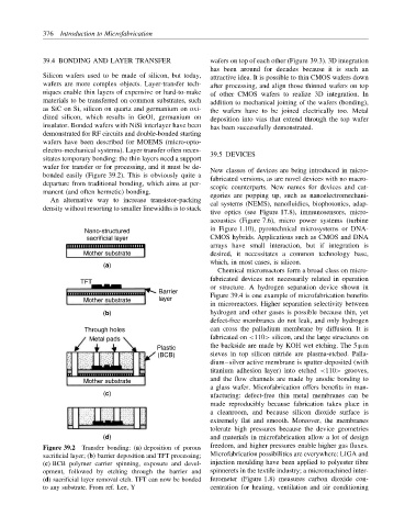
Nano-structured in Figure 1.10), pyrotechnical microsystems or DNA-
sacrificial layer CMOS hybrids. Applications such as CMOS and DNA
arrays have small interaction, but if integration is
Mother substrate desired, it necessitates a common technology base,
(a) which, in most cases, is silicon.
Chemical microreactors form a broad class on micro-
TFT fabricated devices not necessarily related in operation
or structure. A hydrogen separation device shown in
Barrier
Mother substrate layer Figure 39.4 is one example of microfabrication benefits
in microreactors. Higher separation selectivity between
(b) hydrogen and other gases is possible because thin, yet
defect-free membranes do not leak, and only hydrogen
Through holes can cross the palladium membrane by diffusion. It is
Metal pads fabricated on <110> silicon, and the large structures on
Plastic the backside are made by KOH wet etching. The 5 µm
(BCB) sieves in top silicon nitride are plasma-etched. Palla-
dium–silver active membrane is sputter-deposited (with
titanium adhesion layer) into etched <110> grooves,
Mother substrate and the flow channels are made by anodic bonding to
a glass wafer. Microfabrication offers benefits in man-
(c) ufacturing: defect-free thin metal membranes can be
made reproducibly because fabrication takes place in
a cleanroom, and because silicon dioxide surface is
extremely flat and smooth. Moreover, the membranes
tolerate high pressures because the device geometries
(d) and materials in microfabrication allow a lot of design
Figure 39.2 Transfer bonding: (a) deposition of porous freedom, and higher pressures enable higher gas fluxes.
sacrificial layer; (b) barrier deposition and TFT processing; Microfabrication possibilities are everywhere: LIGA and
(c) BCB polymer carrier spinning, exposure and devel- injection moulding have been applied to polyester fibre
opment, followed by etching through the barrier and spinnerets in the textile industry; a micromachined inter-
(d) sacrificial layer removal etch. TFT can now be bonded ferometer (Figure 1.8) measures carbon dioxide con-
to any substrate. From ref. Lee, Y centration for heating, ventilation and air conditioning