
Page 396 - Sami Franssila Introduction to Microfabrication
P. 396
Microfabrication at Large 375
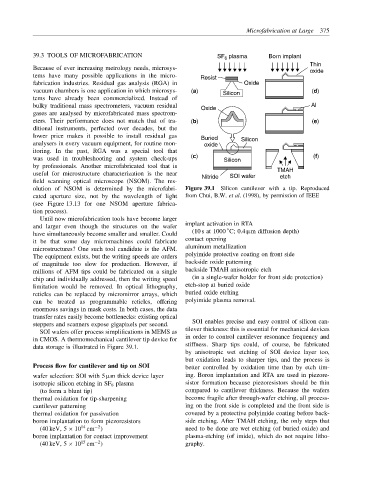
39.3 TOOLS OF MICROFABRICATION SF plasma Born implant
6
Thin
Because of ever increasing metrology needs, microsys- oxide
tems have many possible applications in the micro- Resist
fabrication industries. Residual gas analysis (RGA) in Oxide
vacuum chambers is one application in which microsys- (a) Silicon (d)
tems have already been commercialized. Instead of
bulky traditional mass spectrometers, vacuum residual Oxide Al
gases are analysed by microfabricated mass spectrom-
eters. Their performance does not match that of tra- (b) (e)
ditional instruments, perfected over decades, but the
lower price makes it possible to install residual gas Buried Silicon
analysers in every vacuum equipment, for routine mon- oxide
itoring. In the past, RGA was a special tool that
was used in troubleshooting and system check-ups (c) Silicon (f)
by professionals. Another microfabricated tool that is TMAH
useful for microstructure characterization is the near Nitride SOI wafer etch
field scanning optical microscope (NSOM). The res-
olution of NSOM is determined by the microfabri- Figure 39.1 Silicon cantilever with a tip. Reproduced
cated aperture size, not by the wavelength of light from Chui, B.W. et al. (1998), by permission of IEEE
(see Figure 13.13 for one NSOM aperture fabrica-
tion process).
Until now microfabrication tools have become larger
and larger even though the structures on the wafer implant activation in RTA
◦
have simultaneously become smaller and smaller. Could (10 s at 1000 C; 0.4 µm diffusion depth)
it be that some day micromachines could fabricate contact opening
microstructures? One such tool candidate is the AFM. aluminum metallization
The equipment exists, but the writing speeds are orders polyimide protective coating on front side
of magnitude too slow for production. However, if backside oxide patterning
millions of AFM tips could be fabricated on a single backside TMAH anisotropic etch
chip and individually addressed, then the writing speed (in a single-wafer holder for front side protection)
limitation would be removed. In optical lithography, etch-stop at buried oxide
reticles can be replaced by micromirror arrays, which buried oxide etching
can be treated as programmable reticles, offering polyimide plasma removal.
enormous savings in mask costs. In both cases, the data
transfer rates easily become bottlenecks: existing optical
SOI enables precise and easy control of silicon can-
steppers and scanners expose gigapixels per second.
tilever thickness: this is essential for mechanical devices
SOI wafers offer process simplifications in MEMS as
in CMOS. A thermomechanical cantilever tip device for in order to control cantilever resonance frequency and
data storage is illustrated in Figure 39.1. stiffness. Sharp tips could, of course, be fabricated
by anisotropic wet etching of SOI device layer too,
but oxidation leads to sharper tips, and the process is
Process flow for cantilever and tip on SOI better controlled by oxidation time than by etch tim-
wafer selection: SOI with 5 µm thick device layer ing. Boron implantation and RTA are used in piezore-
isotropic silicon etching in SF 6 plasma sistor formation because piezoresistors should be thin
(to form a blunt tip) compared to cantilever thickness. Because the wafers
thermal oxidation for tip-sharpening become fragile after through-wafer etching, all process-
cantilever patterning ing on the front side is completed and the front side is
thermal oxidation for passivation covered by a protective polyimide coating before back-
boron implantation to form piezoresistors side etching. After TMAH etching, the only steps that
14
−2
(40 keV, 5 × 10 cm ) need to be done are wet etching (of buried oxide) and
boron implantation for contact improvement plasma-etching (of imide), which do not require litho-
−2
15
(40 keV, 5 × 10 cm ) graphy.