
Page 391 - Sami Franssila Introduction to Microfabrication
P. 391
370 Introduction to Microfabrication
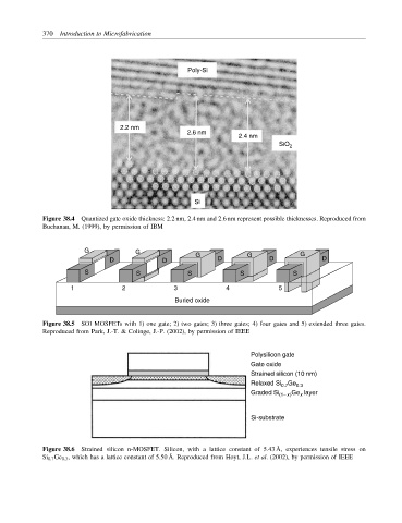
Poly-Si
2.2 nm
2.6 nm
2.4 nm
SiO 2
Si
Figure 38.4 Quantized gate oxide thickness: 2.2 nm, 2.4 nm and 2.6 nm represent possible thicknesses. Reproduced from
Buchanan, M. (1999), by permission of IBM
G G G G G
D D D D D
S S S S S
1 2 3 4 5
Buried oxide
Figure 38.5 SOI MOSFETs with 1) one gate; 2) two gates; 3) three gates; 4) four gates and 5) extended three gates.
Reproduced from Park, J.-T. & Colinge, J.-P. (2002), by permission of IEEE
Polysilicon gate
Gate oxide
Strained silicon (10 nm)
Relaxed Si 0.7 Ge 0.3
Graded Si (1−x) Ge layer
x
Si-substrate
Figure 38.6 Strained silicon n-MOSFET. Silicon, with a lattice constant of 5.43 ˚ A, experiences tensile stress on
Si 0.7 Ge 0.3 , which has a lattice constant of 5.50 ˚ A. Reproduced from Hoyt, J.L. et al. (2002), by permission of IEEE