
Page 386 - Sami Franssila Introduction to Microfabrication
P. 386
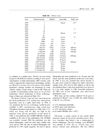
Moore’s Law 365


                                            Table 38.1 Moore’s law
                          Year     Transistors/chip  DRAM     Linewidth  Wafer size
                          1959                1                30 µm        0.5 ′′
                          1960                2
                          1961                4
                          1962                8                             1 ′′
                          1963               16
                          1964               32                20 µm        1.5 ′′
                          1965               64
                          1968              256                12 µm        2 ′′
                          1970             1024      1 k       8 µm
                          1973             4096      4 k       5 µm
                          1975            16 384     16 k      3 µm         3 ′′
                          1979            65 536     64 k      2 µm
                          1983           262 144    256 k      1.5 µm    100 mm
                          1986          1 048 576    1 M       1.2 µm    125 mm
                          1989          4 194 304    4 M       0.8 µm    150 mm
                          1992         16 777 216   16 M       0.5 µm
                          1995         67 108 864   64 M      0.35 µm    200 mm
                          1998        268 435 456  256 M      0.25 µm
                          2000        536 870 912  512 M      0.18 µm
                          2002       1 073 741 824   1 G      0.13 µm    300 mm
                          2004       2 147 483 648   2 G       90 nm
                          2006       4 294 967 296   4 G       65 nm
                          2008       8 589 934 592   8 G       45 nm
                          2010      17 179 869 184  16 G       32 nm


           to continue at a regular pace. Devices are now being  lithography has been predicted to be 10 years into the
           designed with different criteria according to their power  future, and this same prediction holds true even today.
           consumption: in high performance (HP) systems, gate  In 1989, it was also assumed that silicon dioxide as
           oxide is aggressively scaled down and leakage currents  the gate oxide would be replaced by high-k dielectrics
           are allowed to increase, but in low power (LP) portable  starting from 1993, but in 2003 high-k is still in the
           electronics, leakage currents are minimized by using  development phase. Long-term predictions have been off
           ‘thicker’ oxides: 2.4 nm versus 1.3 nm for HP. There are  by a far wider margin: in 1984, linewidth predictions
           a number of demanding scaling issues as we go from  for 2007 were 0.1 µm (optimistic case) and 0.5 µm
           established 130 nm technology to 65 nm technology.  (pessimistic case).
           Some of these are collected in Table 38.2.    How long can this scaling continue? If all goes as
             The death of Moore’s law has been much discussed  predicted by Moore’s law, in 2059, the 100th birthday
           but newer predictions of IC scaling have often proven  of the IC, we will have:
           inaccurate, even in a quite short term: in 1994, it
           was predicted that 0.1 µm technology would become  • 2.5 ˚ A minimum linewidth;
           available in 2007, microprocessor chips would have  • 0.04 ˚ A gate oxide thickness;
           350 million transistors and operate at 1 GHz with 1.2 V,  • 2 mV operating voltage;
                                                                               18
           which was wrong with the date, too high on the  • 64 exabit DRAMs (exa = 10 ).
           transistor count and too pessimistic on the speed. In
           1986, it was predicted that 16 Mbit DRAMs would be  Obviously, a scaled version of the current MOS
           available at the turn of the millennium, but 256 Mbit  transistor cannot be the device described above. How-
           was available. Around 1980, the prediction was that  ever, remember that Moore’s law is independent of
           optical lithography could not print lines smaller than  device technology. The first working 1 µm MOSFET
           1 µm and in 1989, the end of optical lithography was  was reported in 1974, and ca. 15 years later 1 µm
           predicted for 1997. Quite regularly, the end of optical  devices entered mass production. The first 100 nm