
Page 381 - Sami Franssila Introduction to Microfabrication
P. 381
360 Introduction to Microfabrication
3. Maskless lithography by direct writing is expen-
50 Total sive because it is very slow, but there is no pho-
D ≈ 0.3/cm 2
o
40 (1992) tomask cost. Assuming identical capital investment
($6 million) and running costs ($0.5 million/year) for
Cost ($/cm 2 ) 30 both optical and direct write lithography systems (a
very crude approximation), and 100 WPH for optical
20 1.3 cm 2 and 2 WPH for DW on 300 mm wafers, what would
be the number of wafers at which DW becomes com-
Proc.
10 petitive with optical lithography for 0.1 µm CMOS
Waste Package if the mask set cost is assumed to be $500 000?
0 4. If photoresist stripping in a 30 000 WPM fab is 50/50
0.1 1 10 100 1000 between wet tanks and single-wafer plasma strippers,
2
Area (cm ) how many wet benches and plasma strip tools are
(a) needed? Make assumptions about throughputs based
on similar processes/tools.
5. If a 30 000 WPM fab has four gate oxidation tubes,
50 what is their average utilization?
15
Total 6. Under the conditions of 10 cm −2 phosphorus
40 implant dose, 200 mm wafer size, PH 3 bottle vol-
Cost ($/cm 2 ) 30 D o ≈ 0.3 cm −2 D o ≈ 0.01 cm −2 ume 3 L (STP), how many wafers can be implanted?
If ion current is 1 mA, what is the interval for bot-
(1992)
tle changing?
20 (2010) 7. If a 2 cm chip has 1000 output pins, what would be
2
13 cm 2
Proc. the pin pitch at the chip periphery if an arrangement
10 such as the one in Figure 37.1 was employed?
Waste Package 8. How many 30 000 WPM fabs are there in the world?
0
0.1 1 10 100 1000
2
Area (cm ) REFERENCES AND RELATED READINGS
(b) Diebold, A.C.: Materials and failure analysis methods and
systems used in the development and manufacture of silicon
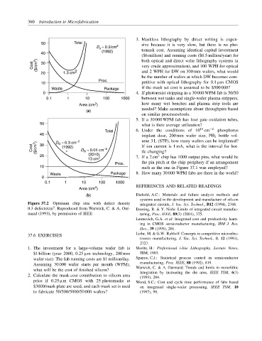
Figure 37.2 Optimum chip size with defect density integrated circuits, J. Vac. Sci. Technol., B12 (1994), 2768.
2
0.3 defects/cm . Reproduced from Warwick, C. & A. Our- Doering, R. & Y. Nishi: Limits of integrated circuit manufac-
mazd (1993), by permission of IEEE turing, Proc. IEEE, 89(3) (2001), 375.
Leonovich, G.A. et al: Integrated cost and productivity learn-
ing in CMOS semiconductor manufacturing, IBM J. Res.
Dev., 39 (1995), 201.
Liehr, M. & G.W. Rubloff: Concepts in competitive microelec-
37.6 EXERCISES
tronics manufacturing, J. Vac. Sci. Technol., B, 12 (1994),
2727.
1. The investment for a large-volume wafer fab is Moritz, H.: Professional i-line Lithography, Lecture Notes,
$1 billion (year 2000, 0.25 µm technology, 200 mm IBM, 1993.
wafer size). The fab running costs are $1 million/day. Spanos, C.J.: Statistical process control in semiconductor
Assuming 30 000 wafer starts per month (WPM), manufacturing, Proc. IEEE, 80 (1992), 819.
what will be the cost of finished silicon? Warwick, C. & A. Ourmazd: Trends and limits in monolithic
integration by increasing the die area, IEEE TSM, 6(3)
2. Calculate the mask-cost contribution to silicon area
(1993), 284.
price if 0.25 µm CMOS with 25 photomasks at Wood, S.C.: Cost and cycle time performance of fabs based
$3000/mask plate are used, and each mask set is used on integrated single-wafer processing, IEEE TSM, 10
to fabricate 50/500/5000/50000 wafers? (1997), 98.