
Page 377 - Sami Franssila Introduction to Microfabrication
P. 377
356 Introduction to Microfabrication
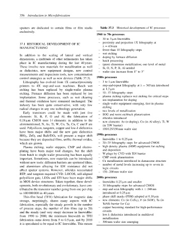
sputters are dedicated to certain films or film stacks Table 37.3 Historical development of IC processes
exclusively.
1960 to 70s processes
– 30 to 3 µm linewidths
– proximity and projection 1X lithography at
37.1 HISTORICAL DEVELOPMENT OF IC
MANUFACTURING λ = 436 nm
– fewer than 10 lithography steps
– wet etching
In addition to the scaling of lateral and vertical – doping by furnace diffusion
dimensions, a multitude of other refinements has taken – batch processing
place in IC manufacturing during the last 40 years. – (pure) aluminium metallization; one level of metal
These involve new materials for metallization as well – Si, O, N, P, B, Al needed
as dielectrics, new equipment designs, new control – wafer size increase from 1” to 3”
measurements and inspections tools, new contamination
control strategies as well as new devices (Table 37.3). 1980s processes
Lithography has evolved from 1X contact/proximity – 3 to 1 µm linewidths
printers to 4X step-and-scan machines. Batch wet – step-and-repeat lithography at λ = 365 nm introduced
etching has been replaced by single-wafer plasma at 1.2 µm
etching. Furnace diffusion has been replaced by ion – 10–15 lithography steps
implantation. Some processes, such as wet cleaning – plasma etching replaces wet etching for critical steps
and thermal oxidation have remained unchanged. The – ion implantation for doping
industry has been quite conservative, with very few – single-wafer equipment emerging, first in plasma
radical changes in any one technology generation. etching
Early transistors could be made with just five – two levels of metallization
– SOG and resist etchback planarization
elements: Si, B, P, O and Al; the fabrication of – silicides introduced
0.18 µm CMOS uses 14 elements: in addition to the
– new elements: As (n-doping), Cu (in Al-alloy), Ti, W
aforementioned, N, As, Ti, W, Co, Ta, Cu, C and F are (in TiW barrier)
used. Polysilicon, tungsten, copper and low-k dielectrics – 100/125/150 mm wafer size
have been major shifts and the new gate dielectrics
HfO 2 , ZrO 2 and BaSrTiO 3 will present a major shift 1990s processes
because they are deposited films, unlike thermal oxides, – linewidths 1 to 0.25 µm
which are grown. – 20–25 lithography steps for advanced CMOS
Plasma etching, wafer steppers, CMP and electro- – high density plasma (HDP) equipment for etching
plating have been major tool changes, but the shift and deposition
– W-plugs by CVD with TiN barrier
from batch to single-wafer processing has been equally
– CMP oxide planarization
important. Sometimes, new materials can be introduced
– Cu metallization introduced in damascene structure
without new tools: diffusion barriers are sputtered films,
– number of metal levels increasing up to seven in
and aluminium alloying for EM resistance did not
logic circuits
affect sputter systems. However, silicides necessitated
– 150–200 mm wafer size
RTP, and tungsten required CVD. LOCOS, self-aligned
polysilicon gate, LDDs and STI have been major shifts 2000s processes
in MOS device structures. Taken together, these devel- – linewidths 0.25 µm and smaller
opments, both revolutionary and evolutionary, have con- – 30 lithography steps for advanced CMOS
tributed to the transistor number going from one per chip – step-and-scan lithography with λ = 248 nm
to 100 000 000 in 40 years. introduced at 0.25 µm
Thin-film head (TFH) fabrication for magnetic data – phase shift masks (PSM) adopted at 0.18 µm
storage, surprisingly, shares many aspects with IC – new elements: Co (in CoSi 2 ), F (in SiOF), Ta (in
fabrication, especially the steady growth in the number TaNSi barrier for Cu)
of process steps, the number of thin films (up to 20) – copper becoming standard for high-performance
and the steady (and very steep) decrease in linewidths: circuits
from 1990 to 2000, the minimum linewidth in TFH – low-k dielectrics introduced in multilevel
metallization
fabrication came down from 5 to 0.5 µm, and by 2010 – 300 mm wafer size emerging
it is speculated to be equal to IC linewidths. This means