
Page 376 - Sami Franssila Introduction to Microfabrication
P. 376
37
Wafer Fab
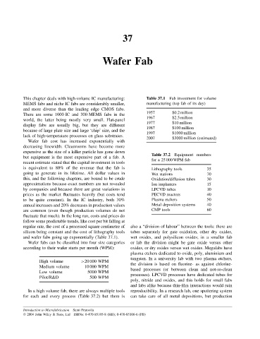
This chapter deals with high-volume IC manufacturing: Table 37.1 Fab investment for volume
MEMS fabs and niche IC fabs are considerably smaller, manufacturing (top fab of its day)
and more diverse than the leading edge CMOS fabs.
There are some 1000 IC and 300 MEMS fabs in the 1957 $0.2 million
world, the latter being mostly very small. Flat-panel 1967 $2.5 million
display fabs are usually big, but they are different 1977 $10 million
$100 million
1987
because of large plate size and large ‘chip’ size, and the 1997 $1000 million
lack of high-temperature processes on glass substrates. 2007 $3000 million (estimated)
Wafer fab cost has increased exponentially with
decreasing linewidth. Cleanrooms have become more
expensive as the size of a killer particle has gone down
but equipment is the most expensive part of a fab. A Table 37.2 Equipment numbers
for a 25 000 WPM fab
recent estimate stated that the capital investment in tools
is equivalent to 80% of the revenue that the fab is Lithography tools 35
going to generate in its lifetime. All dollar values in Wet stations 70
this, and the following chapters, are bound to be crude Oxidation/diffusion tubes 30
approximations because exact numbers are not revealed Ion implanters 15
by companies and because there are great variations in LPCVD tubes 10
prices as the market fluctuates heavily (but costs tend PECVD reactors 40
to be quite constant). In the IC industry, both 30% Plasma etchers 50
annual increases and 20% decreases in production values Metal deposition systems 40
are common (even though production volumes do not CMP tools 60
fluctuate that much). In the long run, costs and prices do
follow some predictable trends, like cost per bit falling at
regular rate, the cost of a processed square centimetre of also a “division of labour” between the tools: there are
silicon being constant and the cost of lithography tools tubes separately for gate oxidation, other dry oxides,
and wafer fabs going up exponentially (Table 37.1). wet oxides, and polysilicon oxides; in a smaller fab
Wafer fabs can be classified into four size categories or lab the division might be gate oxide versus other
according to their wafer starts per month (WPM): oxides, or dry oxides versus wet oxides. Megafabs have
plasma etchers dedicated to oxide, poly, aluminium and
tungsten. In a university lab with two plasma etchers,
High volume >20 000 WPM the division is based on fluorine- as against chlorine-
Medium volume 10 000 WPM based processes (or between clean and not-so-clean
Low volume 5000 WPM processes). LPCVD processes have dedicated tubes for
Pilot/R&D 500 WPM
poly, nitride and oxides, and this holds for small fabs
and labs alike because thin-film interactions would ruin
In a high volume fab, there are always multiple tools reproducibility. In a research lab, one sputtering system
for each and every process (Table 37.2) but there is can take care of all metal depositions, but production
Introduction to Microfabrication Sami Franssila
2004 John Wiley & Sons, Ltd ISBNs: 0-470-85105-8 (HB); 0-470-85106-6 (PB)