
Page 380 - Sami Franssila Introduction to Microfabrication
P. 380
Wafer Fab 359
Labour $1.7/wafer
Consumables (resist, etc.) $2/wafer
Operation (electricity, etc.) $0.15/wafer
Total lithography cost is then $8.55/wafer. So far,
100% yield has been assumed but in real life, yield
loss severely affects the actual number of good chips.
Assumptions for yield loss calculation are
200 mm wafer size;
2
350 chips/wafer (0.85 cm );
2
0.01 defects/cm from lithography;
cost of good chip $3.
Systematic loss comes from tails of statistical distri-
butions: 3σ process capability in both alignment and
in linewidth yields 99.4% good chips, or 346 good
chips (0.994 × 0.994 × 350), with four scrap chips.
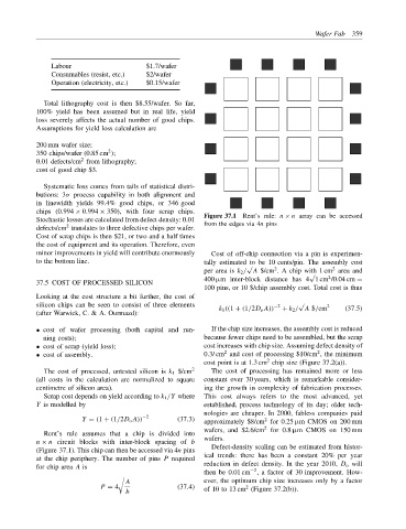
Stochastic losses are calculated from defect density: 0.01 Figure 37.1 Rent’s rule: n × n array can be accessed
from the edges via 4n pins
2
defects/cm translates to three defective chips per wafer.
Cost of scrap chips is then $21, or two and a half times
the cost of equipment and its operation. Therefore, even
minor improvements in yield will contribute enormously Cost of off-chip connection via a pin is experimen-
to the bottom line. tally estimated to be 10 cents/pin. The assembly cost
√
2
2
per area is k 2 / A $/cm . A chip with 1 cm area and
√
2
37.5 COST OF PROCESSED SILICON 400 µm inter-block distance has 4 1 cm /0.04 cm =
100 pins, or 10 $/chip assembly cost. Total cost is thus
Looking at the cost structure a bit further, the cost of
silicon chips can be seen to consist of three elements k 1 ((1 + (1/2D o A)) −2 + k 2 / A $/cm 2 (37.5)
√
(after Warwick, C. & A. Ourmazd):
• cost of wafer processing (both capital and run- If the chip size increases, the assembly cost is reduced
ning costs); because fewer chips need to be assembled, but the scrap
• cost of scrap (yield loss); cost increases with chip size. Assuming defect density of
2
2
• cost of assembly. 0.3/ cm and cost of processing $10/cm , the minimum
2
cost point is at 1.3 cm chip size (Figure 37.2(a)).
The cost of processed, untested silicon is k 1 $/cm 2 The cost of processing has remained more or less
(all costs in the calculation are normalized to square constant over 30 years, which is remarkable consider-
centimetre of silicon area). ing the growth in complexity of fabrication processes.
Scrap cost depends on yield according to k 1 /Y where This cost always refers to the most advanced, yet
Y is modelled by established, process technology of its day; older tech-
nologies are cheaper. In 2000, fabless companies paid
Y = (1 + (1/2D o A)) −2 (37.3) 2
approximately $8/cm for 0.25 µm CMOS on 200 mm
2
wafers, and $2.6/cm for 0.8 µm CMOS on 150 mm
Rent’s rule assumes that a chip is divided into
n × n circuit blocks with inter-block spacing of b wafers.
(Figure 37.1). This chip can then be accessed via 4n pins Defect-density scaling can be estimated from histor-
ical trends: there has been a constant 20% per year
at the chip periphery. The number of pins P required
reduction in defect density. In the year 2010, D o will
for chip area A is
−2
then be 0.01 cm , a factor of 30 improvement. How-
A ever, the optimum chip size increases only by a factor
P = 4 (37.4) of 10 to 13 cm (Figure 37.2(b)).
2
b