
Page 373 - Sami Franssila Introduction to Microfabrication
P. 373
352 Introduction to Microfabrication
are prospective killer defects, but only statistically. Fatal
damage proportion has been set to range from 10 to 20%
in the DRAM yield model, to give a range of yields.
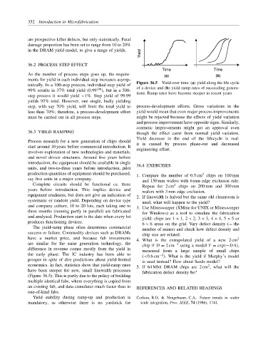
Yield
36.2 PROCESS STEP EFFECT
Time Time
As the number of process steps goes up, the require- (a) (b)
ments for yield in each individual step increases asymp-
totically. In a 100-step process, individual-step yield of Figure 36.5 Yield over time: (a) yield along the life cycle
99% results in 37% total yield (0.99 100 ), but in a 500- of a device and (b) yield-ramp rates of succeeding genera-
tions. Ramp rates have become steeper in recent years
step process it would yield <1%. Step yield of 99.99
yields 95% total. However, one single, badly yielding
step, with say 70% yield, will limit the total yield to process-development efforts. Gross variations in the
less than 70%; therefore, a process-development effort yield would mean that even major process improvements
must be carried out in all process steps. might be rejected because the effects of yield variation
and process improvement have opposite signs. Similarly,
cosmetic improvements might get an approval even
36.3 YIELD RAMPING though the effect came from normal yield variation.
Yield decrease in the end of the lifecycle is real:
Process research for a new generation of chips should
it is caused by process phase-out and decreased
start around 10 years before commercial introduction. It
engineering effort.
involves exploration of new technologies and materials,
and novel device structures. Around five years before
introduction, the equipment should be available in single
units, and two-to-three years before introduction, pilot 36.4 EXERCISES
production quantities of equipment should be purchased, 1. Compare the number of 0.5 cm chips on 100 mm
2
say five units in a major company. and 150 mm wafers with 6 mm edge exclusion rule.
Complete circuits should be functional ca. three Repeat for 2 cm 2 chips on 200 mm and 300 mm
years before introduction. This implies device and wafers with 3 mm edge exclusion.
equipment readiness, but does not give an indication of 2. If linewidth is halved but the same old cleanroom is
systematic or random yield. Depending on device type used, what will happen to the yield?
and company culture, 10 to 20 lots, each taking one to 3. Use Minesweeper (XMine for UNIX or Minesweeper
three months (running partly in parallel) are fabricated for Windows) as a tool to simulate the fabrication
and analysed. Production start is the date when every lot yield: chips are 1 × 1, 2 × 2, 3 × 3, 4 × 4, 5 × 5 or
produces functioning devices. 6 × 6 areas on the grid. Vary defect density (= the
The yield-ramp phase often determines commercial number of mines) and check how defect density and
success or failure. Commodity devices such as DRAMs chip size are related.
have a market price, and because fab investments 4. What is the extrapolated yield of a new 2 cm 2
are similar for the same generation technology, the chip if D = 2 cm −2 using a model Y = exp(−DA),
difference in revenue comes mostly from the yield in measured from a large sample of small chips
the early phase. The IC industry has been able to (<0.6 cm ). What is the yield if Murphy’s model
−2
prosper in spite of dire predictions about yield-limited
is used instead? How about Seeds model?
economics. In fact, statistics show that yield-ramp rates 2
5. If 64 Mbit DRAM chips are 2 cm , what will the
have been steeper for new, small linewidth processes
fabrication defect density be?
(Figure 36.5). This is partly due to the policy of building
multiple identical fabs, where everything is copied from
an existing fab, and data cumulates much faster than in REFERENCES AND RELATED READINGS
one-of-kind fabs.
Yield stability during ramp-up and production is Carlson, R.O. & Neugebauer, C.A.: Future trends in wafer
mandatory, as otherwise there is no yardstick for scale integration, Proc. IEEE, 74 (1986), 1741.