
Page 370 - Sami Franssila Introduction to Microfabrication
P. 370
36
Yield
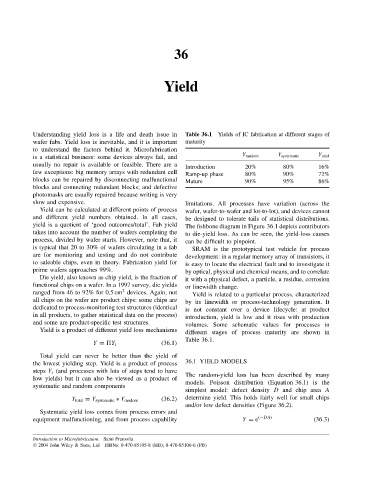
Understanding yield loss is a life and death issue in Table 36.1 Yields of IC fabrication at different stages of
wafer fabs. Yield loss is inevitable, and it is important maturity
to understand the factors behind it. Microfabrication
is a statistical business: some devices always fail, and Y random Y systematic Y total
usually no repair is available or feasible. There are a Introduction 20% 80% 16%
few exceptions: big memory arrays with redundant cell Ramp-up phase 80% 90% 72%
blocks can be repaired by disconnecting malfunctional Mature 90% 95% 86%
blocks and connecting redundant blocks; and defective
photomasks are usually repaired because writing is very
slow and expensive. limitations. All processes have variation (across the
Yield can be calculated at different points of process wafer, wafer-to-wafer and lot-to-lot), and devices cannot
and different yield numbers obtained. In all cases, be designed to tolerate tails of statistical distributions.
yield is a quotient of ‘good outcomes/total’. Fab yield The fishbone diagram in Figure 36.1 depicts contributors
takes into account the number of wafers completing the to die-yield loss. As can be seen, the yield-loss causes
process, divided by wafer starts. However, note that, it can be difficult to pinpoint.
is typical that 20 to 30% of wafers circulating in a fab SRAM is the prototypical test vehicle for process
are for monitoring and testing and do not contribute development: in a regular memory array of transistors, it
to saleable chips, even in theory. Fabrication yield for is easy to locate the electrical fault and to investigate it
prime wafers approaches 99%. by optical, physical and chemical means, and to correlate
Die yield, also known as chip yield, is the fraction of it with a physical defect, a particle, a residue, corrosion
functional chips on a wafer. In a 1997 survey, die yields or linewidth change.
2
ranged from 46 to 92% for 0.5 cm devices. Again, not Yield is related to a particular process, characterized
all chips on the wafer are product chips: some chips are by its linewidth or process-technology generation. It
dedicated to process-monitoring test structures (identical is not constant over a device lifecycle: at product
in all products, to gather statistical data on the process) introduction, yield is low and it rises with production
and some are product-specific test structures. volumes. Some schematic values for processes in
Yield is a product of different yield loss mechanisms different stages of process maturity are shown in
Table 36.1.
Y = Y i (36.1)
Total yield can never be better than the yield of
the lowest yielding step. Yield is a product of process 36.1 YIELD MODELS
steps Y i (and processes with lots of steps tend to have
low yields) but it can also be viewed as a product of The random-yield loss has been described by many
systematic and random components models. Poisson distribution (Equation 36.1) is the
simplest model: defect density D and chip area A
Y total = Y systematic ∗ Y random (36.2) determine yield. This holds fairly well for small chips
and/or low defect densities (Figure 36.2).
Systematic yield loss comes from process errors and
equipment malfunctioning, and from process capability Y = e (−DA) (36.3)
Introduction to Microfabrication Sami Franssila
2004 John Wiley & Sons, Ltd ISBNs: 0-470-85105-8 (HB); 0-470-85106-6 (PB)