
Page 389 - Sami Franssila Introduction to Microfabrication
P. 389
368 Introduction to Microfabrication
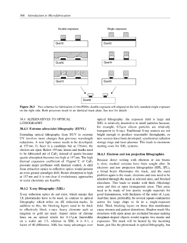
Double exposure Single exposure
Quartz Quartz
Quartz Quartz
Quartz Quartz
Quartz
Figure 38.3 Two schemes for fabrication of rim-PSMs: double exposure self-aligned on the left; standard single exposure
on the right side. Both processes result in an identical mask plate. See text for details
38.4 ALTERNATIVES TO OPTICAL optical lithography: the exposure field is large and
LITHOGRAPHY XRL is relatively insensitive to small particles because,
for example, 0.5 µm silicon particles are relatively
38.4.1 Extreme ultraviolet lithography (EUVL)
transparent to X-rays. Traditional X-ray sources are not
Extending optical lithography from DUV to extreme bright enough to produce reasonable throughputs, so
UV involves more changes than previous wavelength new sources have been developed: synchrotron radiation
reductions. A new light source needs to be developed: storage rings and laser plasmas. This leads to enormous
at 157 nm, F 2 laser is a candidate but at 126 nm, the starting costs for XRL systems.
choices are open. Below 193 nm, lenses and masks need
to be fabricated out of CaF 2 instead of quartz because 38.4.3 Electron and ion projection lithographies
quartz absorption becomes too high at 157 nm. The high
◦ Because direct writing with electron or ion beams
thermal expansion coefficient of 19 ppm/ C of CaF 2
presents major problems with thermal control. A shift is slow, masked versions have been sought after. In
from refractive optics to reflective optics would present electron- and ion- projection lithographies (EPL, IPL),
an even greater paradigm shift. Resist absorption is high a broad beam illuminates the mask, and the main
at 157 nm and it is not clear if evolutionary approaches problem again is the mask: electrons and ions need to be
in resist chemistry are feasible. admitted through the mask at selected sites, and blocked
elsewhere. This leads to masks with thick (blocking)
areas and thin or open (transparent) areas. Thin areas
38.4.2 X-ray lithography (XRL)
need to be made of low atomic weight materials for
X-ray reduction optics do not exist, which means that good transmission, with thickness of the order of 1 µm.
1X photomasks have to be used, in contrast to optical And they must, preferably, be several square centimetres
lithography which relies on 4X reduction masks. In across for large chips to fit in a single-exposure
addition to this, the blocking layers need to be thick field. Thick blocking layers on these thin membranes
to effectively block x-rays: heavy elements such as cause stresses and pattern distortions. Shadow mask-like
tungsten or gold are used. Aspect ratios of chrome structures with open areas are excluded because making
lines on an optical reticle for 0.13 µm linewidths doughnut-shaped objects would require two masks and
on a wafer are 1:5, whereas in XRL it is 8:1, a exposures. The mask will be heated by the incoming
factor of 40 difference. XRL has many advantages over beam, just like the photomask in optical lithography, but