
Page 387 - Sami Franssila Introduction to Microfabrication
P. 387
366 Introduction to Microfabrication
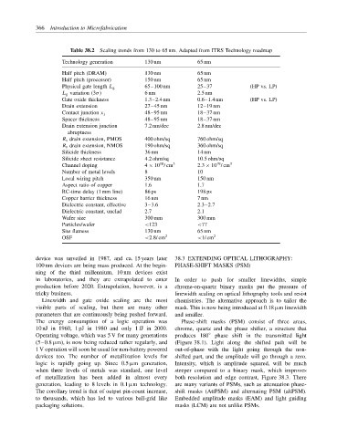
Table 38.2 Scaling trends from 130 to 65 nm. Adapted from ITRS Technology roadmap
Technology generation 130 nm 65 nm
Half pitch (DRAM) 130 nm 65 nm
Half pitch (processor) 150 nm 65 nm
Physical gate length L g 65–100 nm 25–37 (HP vs. LP)
L g variation (3σ) 6 nm 2.5 nm
Gate oxide thickness 1.3–2.4 nm 0.6–1.4 nm (HP vs. LP)
Drain extension 27–45 nm 12–19 nm
48–95 nm 18–37 nm
Contact junction x j
Spacer thickness 48–95 nm 18–37 nm
Drain extension junction 7.2 nm/dec 2.8 nm/dec
abruptness
R s drain extension, PMOS 400 ohm/sq 760 ohm/sq
R s drain extension, NMOS 190 ohm/sq 360 ohm/sq
Silicide thickness 36 nm 14 nm
Silicide sheet resistance 4.2 ohm/sq 10.5 ohm/sq
19
18
Channel doping 4 × 10 / cm 3 2.3 × 10 / cm 3
Number of metal levels 8 10
Local wiring pitch 350 nm 150 nm
Aspect ratio of copper 1.6 1.7
RC-time delay (1 mm line) 86 ps 198 ps
Copper barrier thickness 16 nm 7 nm
Dielectric constant, effective 3–3.6 2.3–2.7
Dielectric constant, unclad 2.7 2.1
Wafer size 300 mm 300 mm
Particles/wafer <123 <77
Site flatness 130 nm 65 nm
OSF <2.8/ cm 2 <1/ cm 2
device was unveiled in 1987, and ca. 15 years later 38.3 EXTENDING OPTICAL LITHOGRAPHY:
100 nm devices are being mass produced. At the begin- PHASE-SHIFT MASKS (PSM)
ning of the third millennium, 10 nm devices exist
in laboratories, and they are extrapolated to enter In order to push for smaller linewidths, simple
production before 2020. Extrapolation, however, is a chrome-on-quartz binary masks put the pressure of
tricky business. linewidth scaling on optical lithography tools and resist
Linewidth and gate oxide scaling are the most chemistries. The alternative approach is to tailor the
visible parts of scaling, but there are many other mask. This is now being introduced at 0.18 µm linewidth
parameters that are continuously being pushed forward. and smaller.
The energy consumption of a logic operation was Phase-shift masks (PSM) consist of three areas,
10 nJ in 1960, 1 pJ in 1980 and only 1 fJ in 2000. chrome, quartz and the phase shifter, a structure that
Operating voltage, which was 5 V for many generations produces 180 ◦ phase shift in the transmitted light
(5–0.8 µm), is now being reduced rather regularly, and (Figure 38.1). Light along the shifted path will be
1 V operation will soon be usual for non-battery powered out-of-phase with the light going through the non-
devices too. The number of metallization levels for shifted part, and the amplitude will go through a zero.
logic is rapidly going up. Since 0.5 µm generation, Intensity, which is amplitude squared, will be much
when three levels of metals was standard, one level steeper compared to a binary mask, which improves
of metallization has been added in almost every both resolution and edge contrast, Figure 38.3. There
generation, leading to 8 levels in 0.1 µm technology. are many variants of PSMs, such as attenuation phase-
The corollary trend is that of output pin-count increase, shift masks (AttPSM) and alternating PSM (altPSM).
to thousands, which has led to various ball-grid like Embedded amplitude masks (EAM) and light guiding
packaging solutions. masks (LCM) are not unlike PSMs.