
Page 395 - Sami Franssila Introduction to Microfabrication
P. 395
374 Introduction to Microfabrication
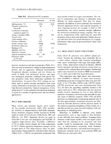
Table 39.1 Diamond and SiC properties need careful control of oxygen concentration. The con-
trol of composition and structure is inherently more
Diamond 3C-SiC difficult for multi-component films than for binary
materials. In addition, in active materials, the correlation
◦
Melting point ( C) 3550 2830
Thermal conductivity 20 5 between deposition process and material properties is
(W/cm K) more important because, for example, in ZnO or AlN
Coefficient of thermal 1 3 piezoelectrics, the crystal structure strongly influences
expansion (ppm/ C) the electrical-to-mechanical energy coupling. This can-
◦
Young’s modulus (GPa) 1200 700 not be compromised while optimizing the usual film
Poisson ratio 0.2 properties such as stress and uniformity. Further process-
Yield strength (GPa) 53 21 ing with these films also entails limitations; for example,
Friction coefficient 0.03 ferroelectric films must be processed below their Curie
Sound velocity (m/s) 18 000 15 000 temperature.
Resistivity (ohm-cm) <10 16
Bandgap (eV) 5.45 2.2
2
Mobility (cm /Vs) 4500
Dielectric constant 5.5 9.72 39.2 HIGH ASPECT RATIO STRUCTURES
Optical transparency (nm) 225– > IR
Refractive index 2.41 Early silicon IC processes were dubbed ‘planar pro-
cesses’ because the structures were essentially flat on
(at 591 nm)
a wafer surface, whereas older transistor technologies
were ‘mesa’ technologies with large step height differ-
thermal, mechanical and optical properties (Table 39.1). ences. Today, deep-trench isolation in bipolars, DRAM
They are used as protective coatings in high-temperature trench capacitors and deep sub-micron contact holes are
devices and in aggressive chemical environments. common in ICs, making them all but planar. Similar high
Exceptional abrasion resistance and low friction are aspect ratio structures are found in DRIE micromechan-
useful in fluidic and mechanical devices, and supe- ics, in LIGA and in thin-film head fabrication.
rior mechanical properties combined with special sur- Film deposition into high aspect ratio microstruc-
face properties make them interesting candidates for tures (HARMS) is difficult. As aspect ratio increases,
microswitches. As passive films, DLC coatings are rou- maintaining good step coverage becomes even more dif-
tinely used to protect moving mechanical parts from ficult. A few CVD films (TEOS oxide, LPCVD nitride,
contact. Diamond is an insulator, but it has exceptionally LPCVD polysilicon) and some electrodeposited films
high thermal conductivity. Optical transparency of dia- (Cu, Ni) have the gap-filling capability needed to fill
mond from UV to IR combined with electrical insulation aspect ratios up to 100:1. Deposition into any structure
is useful for a number of optoelectronic and microfluidic usually involves deposition on two or more different
applications. materials: for instance, the bottom and sidewalls are usu-
ally made of different materials. PVD, CVD and ECD
processes are independent of underlying material only in
39.1.2 Active materials the first approximation: nucleation processes are influ-
enced by both the chemical and the physical nature of
Many sensors and actuators require active materi- the surfaces in question (roughness, texture, bonds, etc.),
als, for example, piezoelectric (ZnO, AlN), pyroelec- and film growth rate, grain size and roughness will vary
tric (LiTaO 3 ) or magnetostrictive (FeCoSiB) materials. depending on underlying films.
Future memories (magnetic RAM, ferroelectric RAM) Metrology of HARMS is difficult: even simple
might be made of ferroelectrics (SrBi 2 Ta 2 O 9 , SBT and measurements, such as step height or film thickness
PbZr x Ti 1−x O 3 , PZT). Spintronic devices are made in on the sidewall, pose major problems. Scanning probe
GaAs:Mn (a few per cent manganese) and GaN:Mn. In methods would require needles with even higher aspect
magnetic shape-memory alloy, Ni 2 GaMn, a difference ratios than the structures to be measured, and such
of 2% in nickel content changes the Curie temperature needles would be mechanically weak. Optical beams
◦
by 50 C. Similar operating-temperature changes can be (e.g., in interferometry) necessitate beam diameters
brought about in TiNi shape-memory alloys by palla- smaller than the structures, and small beam divergences.
dium doping. Superconductors with perovskite structure Destructive methods such as cross-sectional SEM and
(YBa 2 Cu 3 O 7−δ , YBCO), are quaternary compounds that TEM must be used quite often.