
Page 398 - Sami Franssila Introduction to Microfabrication
P. 398
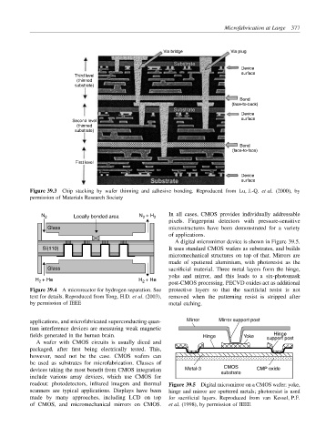
Microfabrication at Large  377


                                                     Via bridge            Via plug

                                                                              Device
                                                                              surface
                         Third level
                         (thinned
                         substrate)
                                                                              Bond
                                                                           (face-to-back)
                                                                              Device
                        Second level                                          surface
                         (thinned
                         substrate)
                                                                              Bond
                                                                           (face-to-face)
                         First level
                                                                              Device
                                                                              surface

           Figure 39.3 Chip stacking by wafer thinning and adhesive bonding. Reproduced from Lu, J.-Q. et al. (2000), by
           permission of Materials Research Society

              N 2        Locally bonded area  N + H 2  In all cases, CMOS provides individually addressable
                                               2
                                                       pixels. Fingerprint detectors with pressure-sensitive
                Glass                                  microstructures have been demonstrated for a variety
                                                       of applications.
                                                         A digital micromirror device is shown in Figure 39.5.
               Si(110)                                 It uses standard CMOS wafers as substrates, and builds
                                                       micromechanical structures on top of that. Mirrors are
                                                       made of sputtered aluminium, with photoresist as the
                Glass                                  sacrificial material. Three metal layers form the hinge,
                                                       yoke and mirror, and this leads to a six-photomask
            H + He                           H + He
             2
                                              2
                                                       post-CMOS processing. PECVD oxides act as additional
           Figure 39.4 A microreactor for hydrogen separation. See  protective layers so that the sacrificial resist is not
           text for details. Reproduced from Tong, H.D. et al. (2003),  removed when the patterning resist is stripped after
           by permission of IEEE                       metal etching.

           applications, and microfabricated superconducting quan-  Mirror  Mirror support post
           tum interference devices are measuring weak magnetic
                                                                                        Hinge
           fields generated in the human brain.                    Hinge        Yoke   support post
             A wafer with CMOS circuits is usually diced and
           packaged, after first being electrically tested. This,
           however, need not be the case. CMOS wafers can
           be used as substrates for microfabrication. Classes of
                                                                        CMOS
           devices taking the most benefit from CMOS integration  Metal-3  substrate  CMP oxide
           include various array devices, which use CMOS for
           readout: photodetectors, infrared imagers and thermal  Figure 39.5 Digital micromirror on a CMOS wafer: yoke,
           scanners are typical applications. Displays have been  hinge and mirror are sputtered metals; photoresist is used
           made by many approaches, including LCD on top  for sacrificial layers. Reproduced from van Kessel, P.F.
           of CMOS, and micromechanical mirrors on CMOS.  et al. (1998), by permission of IEEE