
Page 174 - MEMS and Microstructures in Aerospace Applications
P. 174
Osiander / MEMS and microstructures in Aerospace applications DK3181_c008 Final Proof page 164 1.9.2005 12:05pm
164 MEMS and Microstructures in Aerospace Applications
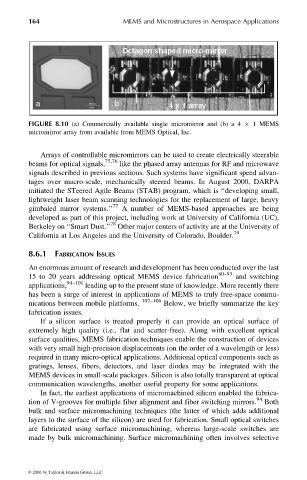
FIGURE 8.10 (a) Commercially available single micromirror and (b) a 4 1 MEMS
micromirror array from available from MEMS Optical, Inc.
Arrays of controllable micromirrors can be used to create electrically steerable
75,76
beams for optical signals, like the phased array antennas for RF and microwave
signals described in previous sections. Such systems have significant speed advan-
tages over macro-scale, mechanically steered beams. In August 2000, DARPA
initiated the STeered Agile Beams (STAB) program, which is ‘‘developing small,
lightweight laser beam scanning technologies for the replacement of large, heavy
gimbaled mirror systems.’’ 77 A number of MEMS-based approaches are being
developed as part of this project, including work at University of California (UC),
78
Berkeley on ‘‘Smart Dust.’’ Other major centers of activity are at the University of
California at Los Angeles and the University of Colorado, Boulder. 79
8.6.1 FABRICATION ISSUES
An enormous amount of research and development has been conducted over the last
15 to 20 years addressing optical MEMS device fabrication 80–93 and switching
applications, 94–101 leading up to the present state of knowledge. More recently there
has been a surge of interest in applications of MEMS to truly free-space commu-
nications between mobile platforms. 102–106 Below, we briefly summarize the key
fabrication issues.
If a silicon surface is treated properly it can provide an optical surface of
extremely high quality (i.e., flat and scatter-free). Along with excellent optical
surface qualities, MEMS fabrication techniques enable the construction of devices
with very small high-precision displacements (on the order of a wavelength or less)
required in many micro-optical applications. Additional optical components such as
gratings, lenses, fibers, detectors, and laser diodes may be integrated with the
MEMS devices in small-scale packages. Silicon is also totally transparent at optical
communication wavelengths, another useful property for some applications.
In fact, the earliest applications of micromachined silicon enabled the fabrica-
tion of V-grooves for multiple fiber alignment and fiber switching mirrors. 94 Both
bulk and surface micromachining techniques (the latter of which adds additional
layers to the surface of the silicon) are used for fabrication. Small optical switches
are fabricated using surface micromachining, whereas large-scale switches are
made by bulk micromachining. Surface micromachining often involves selective
© 2006 by Taylor & Francis Group, LLC