
Page 183 - MEMS and Microstructures in Aerospace Applications
P. 183
Osiander / MEMS and microstructures in Aerospace applications DK3181_c008 Final Proof page 173 1.9.2005 12:05pm
Microelectromechanical Systems for Spacecraft Communications 173
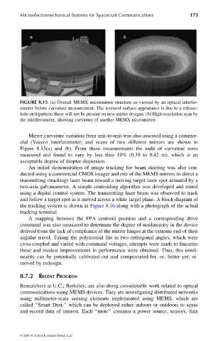
FIGURE 8.15 (a) Overall MEMX micromirror structure as viewed by an optical interfer-
ometer before curvature measurement. The textured surface appearance is due to a release-
hole etch pattern; these will not be present on new mirror designs. (b) High-resolution scan by
the interferometer, showing curvature of another MEMX micromirror.
Mirror curvature variation from unit-to-unit was also assessed using a commer-
cial (Veeco) interferometer, and scans of two different mirrors are shown in
Figure 8.15(a) and (b). From these measurements the radii of curvature were
measured and found to vary by less than 10% (0.39 to 0.42 m), which is an
acceptable degree of diopter dispersion.
An initial demonstration of image tracking for beam steering was also con-
ducted using a commercial CMOS imager and one of the MEMS mirrors to direct a
transmitting (tracking) laser beam toward a moving target laser spot actuated by a
two-axis galvanometer. A simple centroiding algorithm was developed and tested
using a digital control system. The transmitting laser beam was observed to track
and follow a target spot as it moved across a white target plane. A block diagram of
the tracking system is shown in Figure 8.16 along with a photograph of the actual
tracking terminal.
A mapping between the FPA centroid position and a corresponding drive
command was also measured to determine the degree of nonlinearity in the device
derived from the lack of compliance of the mirror hinges at the extreme end of their
angular travel. Taking the polynomial fits in two orthogonal angles, which were
cross-coupled and varied with command voltages, attempts were made to linearize
these and modest improvements in performance were obtained. Thus, this nonli-
nearity can be potentially calibrated-out and compensated-for, or, better yet, re-
moved by redesign.
8.7.2 RECENT PROGRESS
Researchers at U.C., Berkeley, are also doing considerable work related to optical
communications using MEMS devices. They are investigating distributed networks
using millimeter-scale sensing elements implemented using MEMS, which are
called ‘‘Smart Dust,’’ which can be deployed either indoors or outdoors to sense
and record data of interest. Each ‘‘mote’’ contains a power source, sensors, data
© 2006 by Taylor & Francis Group, LLC