
Page 184 - MEMS and Microstructures in Aerospace Applications
P. 184
Osiander / MEMS and microstructures in Aerospace applications DK3181_c008 Final Proof page 174 1.9.2005 12:05pm
174 MEMS and Microstructures in Aerospace Applications
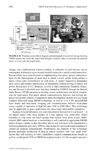
Target Sub-window
field coverage
Target beam
(670 nm)
Target beam (635 nm)
Galvanometer
Beam
splitter
MEMS
micro-minor
Dichroic
fitter
Collimator Camera Collimator
lens
Tip/tilt CMOS Laser
voltage Laser camera
Function
generator
Leg 1-2-3 voltages
USB2
High-speed DSP/FPGA DSP MatLab Simulink CMDS
DAC board board Ethernet system camera
driver Centroid code driver
DSP/FPGA system Personal computer
FIGURE 8.16 Tracking-system block diagram and photograph of actual test set-up, showing
CMOS camera that views the target field through a dichroic filter to eliminate the tracking
beam so it sees only the target beam.
storage, and a bidirectional wireless modem. A collection of such devices can be
interrogated at distances up to several hundred meters by a small central transceiver.
Recent efforts have been focused on implementing free-space optical communica-
tions for the interrogation of smart dust in which a novel uplink design utilizes a
micro corner-cube retroreflector on each mote. A central transceiver illuminates
these motes and permits transmission of information without having to radiate any
power. Researchers at UC, Berkeley, as well as other institutions (Stanford, Prince-
ton, and Sensors Unlimited) have also been funded by DARPA through the Steered
Agile Beams (STAB) program to develop system architectures and novel compon-
ents for high-speed, free-space optical communication between fast-moving air-
planes and ground vehicles. Components under development include two-axis beam
scanners fabricated using MEMS technology, as well as (1 to 5 W) InGaAsP/InP
laser diodes and dual-mode (imaging and communication) InGaAs focal-plane
arrays capable of operation at high bit rates (100 to 1000 Mbs). This technology
may be applicable to space applications for close-range intersatellite operations.
Scaling of recent laboratory test units described in Section 8.6.1 to at least 4 4
(or larger) arrays with array pitches of 2 mm appears very achievable, which
translates to chip areas not much greater than typical focal plane arrays. Multi-
channel DSP control hardware is needed that is well-matched to appropriate MEMS
mirror designs (similar to that described above) and will need to be translated to a
field programmable gate array (FPGA) chip design for spacecraft implementation to
control all elements independently. Furthermore, the maturity of this technology
permits prototype production of plug-in optical modules with very small form-
factors that will interface to both a multifiber coupled communications bundle as
well as a multi-point CCD or CMOS focal plane tracker. A 1-D concept to upscale a
© 2006 by Taylor & Francis Group, LLC