
Page 349 -
P. 349
X-Ray–Based Fabrication 5-11
12.5 cm 5 cm. This may be compared to the time (depending on storage ring beam current) of roughly
20 to 30 minutes needed to perform the same area exposure at 250 µm thickness using 1.5 GeV CAMD
bending magnet radiation. The enhanced high energy performance results in a throughput for a 250µm
PMMA thickness of over 200 substrates per day per beamline. The result reveals a practical approach for
direct LIGA with the use of PMMA or using DXRL as the primary tool for precision mold fabrication.
Similar opportunities exist for the negative chemically amplified X-ray resists, and convenient batch X-
ray exposure end-stations ultimately will help to enable higher throughput.
5.2.4 Development
2
Although PMMA sensitivity, at roughly 500 mJ/cm , is much lower than other photoresists, the combina-
tion of high-intensity well-collimated X-ray flux and the existence of a highly selective PMMA developing
system together facilitate exploitation of the high resolution of PMMA in a batch process for obtaining
microminiature ultraprecision molds.A developer composed of an aqueous mixture of solvents (80% dieth-
ylene glycol monobutyl ether, 20% morpholine, 5% ethanolamine, and 15% water), commonly referred
to as the G–G developer after its patent holders, has been formulated to achieve very high contrast PMMA
development [Ghica and Glashauser, 1983; Stutz, 1986]. The G–G developer is typically used at a temper-
ature of 35°C, but may be also used successfully at temperatures down to 15°C with decreased development
rates yet higher selectivity. The G–G developer solution also etches copper, which may require a protective
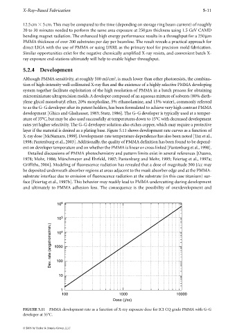
layer if the material is desired as a plating base. Figure 5.11 shows development rate curves as a function of
X-ray dose [McNamara, 1999]. Development-rate temperature dependence has also been noted [Tan et al.,
1998; Pantenburg et al., 2003]. Additionally, the quality of PMMA definition has been found to be depend-
ent on developer temperature and on whether the PMMA is linear or cross-linked [Pantenburg et al., 1998].
Detailed discussions of PMMA photochemistry and pattern limits exist in several references [Ouano,
1978; Mohr, 1986; Münchmeyer and Ehrfeld, 1987; Pantenburg and Mohr, 1995; Feiertag et al., 1997a;
Griffiths, 2004]. Modeling of fluorescence radiation has revealed that a dose of magnitude 500 J/cc may
be deposited underneath absorber regions at areas adjacent to the mask absorber edge and at the PMMA-
substrate interface due to emission of fluorescence radiation at the substrate (in this case titanium) sur-
face [Feiertag et al., 1997b]. This behavior may readily lead to PMMA undercutting during development
and ultimately to PMMA adhesion loss. The consequence is the possibility of overdevelopment and
10 6
10 5 4
Dev. rate (angstroms/min.) 1000
10
100
10
1
100 1000 10000
Dose (j/cc)
FIGURE 5.11 PMMA development rate as a function of X-ray exposure dose for ICI CQ grade PMMA with G–G
developer at 35°C.
© 2006 by Taylor & Francis Group, LLC