
Page 347 -
P. 347
X-Ray–Based Fabrication 5-9
5.2.2 Thick X-ray Photoresist
As with many MEMS technologies,processing is particularly sensitive to internal and process-induced strain
as well as to adhesion issues. The control of these two areas substantially determines DXRL-based man-
ufacturability. Process stability in this regard mostly concerns the application of a thick, stress-free photore-
sist with exceptional adherance to a metallized substrate for electrolytic deposition or other substrate
material that will facilitate further processing. The difficulty in most photoresist application methods is
avoiding large internal tensile stress, which can lead to crazing during development. A number of X-ray
photoresist materials suitable for thick application have been examined [Ehrfeld et al., 1997]. Because it
possesses relatively good mechanical stability and high resolution, PMMA has been the primary X-ray pho-
toresist. The application procedure initially conceived uses direct polymerization with a casting resin [Mohr
et al., 1988]. A cross-linking agent is typically added in the process to further increase the yield strength and
thereby provide additional resistance to crazing. To improve adhesion to a metallized substrate, an adhesion-
promoting chemistry or intermediate layer may be used [Khan Malek et al., 1998a; DeCarlo et al., 1998].
The nearly 20% volume contraction during polymerization results in a tensile-stressed film; this may be
partially alleviated with annealing but cannot be completely avoided due to thermal mismatch with typ-
ical substrate materials that have lower thermal expansion coefficients. The consequences of residual pho-
toresist stress are constraints on component geometry design rules and limits on processing procedures.
An alternative approach uses a precast low-stress PMMA sheet [Guckel et al., 1996a]. In this method,
a linear high-molecular-weight or cross-linked PMMA sheet is used to obtain PMMA plate cutouts com-
mensurate with a particular substrate geometry. Typical sheet thicknesses range from 500µm to 1cm.
These sheet cutouts are then bonded to a metallized substrate by means of a technique with no significant
temperature variation or induced chemical or mechanical perturbation. One well proven technique uses
a thin prespun layer of high-molecular-weight ( 1 million) PMMA combined with the monomer methyl
methacrylate (MMA) as the bonding solvent. A plate of PMMA is placed on the desired substrate with a
spun PMMA layer typically 1 µm thick. MMA applied between the PMMA surfaces wets the interface via
capillary action. Since the diffusion of MMA through PMMA is rapid even at room temperatures, curing
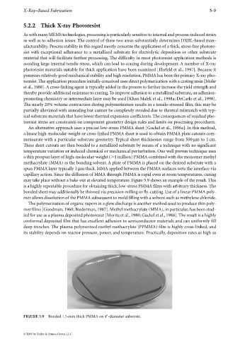
may take place without a bake-out at elevated temperature. Figure 5.9 shows an example of the result. This
is a highly repeatable procedure for obtaining thick, low-stress PMMA films with arbitrary thickness. The
bonded sheet may additionally be thinned via precision milling or fly-cutting. Use of a linear PMMA poly-
mer allows dissolution of the PMMA subsequent to mold filling with a solvent such as methylene chloride.
The polymerization of organic vapors in a glow discharge is another method used to produce thin poly-
mer films [Goodman, 1960; Biederman, 1987]. Methyl methacrylate (MMA), in particular, has been stud-
ied for use as a plasma deposited photoresist [Morita et al., 1980; Guckel et al., 1988]. The result is a highly
conformal deposited film that has excellent adhesion to semiconductor materials and can uniformly fill
deep trenches. The plasma polymerized methyl methacrylate (PPMMA) film is highly cross-linked, and
its stability depends on reactor pressure, power, and temperature. Practically, deposition rates as high as
FIGURE 5.9 Bonded 1.5-mm thick PMMA on 4 -diameter substrate.
© 2006 by Taylor & Francis Group, LLC