
Page 342 -
P. 342
5-4 MEMS: Design and Fabrication
TABLE 5.2 DXRL-Based Processing Attributes
Type of structural Prismatic with arbitrary 2-D shape and sidewall angle
geometry accommodated
Structural thickness Commonly 200–800 microns up to several millimeters (10 centimeters demonstrated)
Lateral run-out 0.1 micron per 100 microns of vertical length
Minimum critical A few microns typical — function of photoresist stability
dimension
Surface roughness 10–20nm RMS typical, as low as several nm
Thickness control With conventional lapping: a few microns typical, as low as 0.5 micron across 4 inch
diameter
Materials Ni, Cu, Au, Ag, NiFe, NiCo, NiFeCo,…
(electroformable metals)
Materials (pressed powders, Alumina, PZT, Ferrites, NdFeB, SmCo, variety of plastics and glasses
embossed, hot forged)
10 5 4
PMMA absorption length ( m) 1000
10
100
10
2 3 4 5 6 7 8 910 20 30
Energy (keV)
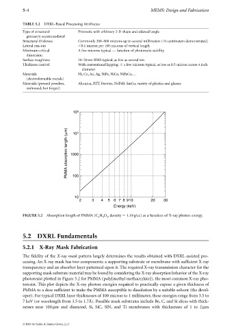
FIGURE 5.2 Absorption length of PMMA (C H O , density 1.19 g/cc) as a function of X-ray photon energy.
5 8 2
5.2 DXRL Fundamentals
5.2.1 X-Ray Mask Fabrication
The fidelity of the X-ray mask pattern largely determines the results obtained with DXRL-assisted pro-
cessing. An X-ray mask has two components: a supporting substrate or membrane with sufficient X-ray
transparency and an absorber layer patterned upon it. The required X-ray transmission character for the
supporting mask substrate material may be found by considering the X-ray absorption behavior of the X-ray
photoresist plotted in Figure 5.2 for PMMA (poly[methyl methacrylate]), the most common X-ray pho-
toresist. This plot depicts the X-ray photon energies required to practically expose a given thickness of
PMMA to a dose sufficient to make the PMMA susceptible to dissolution by a suitable solvent (the devel-
oper). For typical DXRL layer thicknesses of 100 micron to 1 millimeter, these energies range from 3.5 to
7 keV (or wavelength from 3.5 to 1.7Å). Possible mask substrates include Be, C, and Si slices with thick-
nesses near 100µm and diamond, Si, SiC, SiN, and Ti membranes with thicknesses of 1 to 2µm
© 2006 by Taylor & Francis Group, LLC