
Page 341 -
P. 341
X-Ray–Based Fabrication 5-3
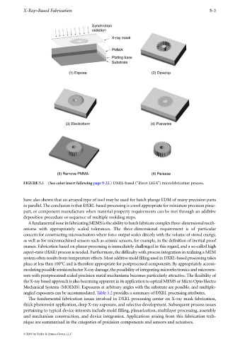
Synchrotron
radiation
X-ray mask
PMMA
Plating base
Substrate
(1) Expose (2) Develop
(3) Electroform (4) Planarize
(5) Remove PMMA (6) Release
FIGURE 5.1 (See color insert following page 9-22.) DXRL-based (“direct LIGA”) microfabrication process.
have also shown that an arrayed type of tool may be used for batch plunge EDM of many precision parts
in parallel. The conclusion is that DXRL-based processing is a tool appropriate for miniature precision piece-
part, or component manufacture when material property requirements can be met through an additive
deposition procedure or sequence of multiple molding steps.
A fundamental issue in fabricating MEMS is the ability to batch fabricate complex three-dimensional mech-
anisms with appropriately scaled tolerances. The three-dimensional requirement is of particular
concern for constructing microactuators where force output scales directly with the volume of stored energy,
as well as for micromachined sensors such as seismic sensors, for example, in the definition of inertial proof
masses. Fabrication based on planar processing is immediately challenged in this regard, and a so-called high
aspect-ratio (HAR) process is needed. Furthermore, the difficulty with process integration in realizing a MEM
system often results from temperature effects. Most additive mold filling used in DXRL-based processing takes
place at less than 100°C and is therefore appropriate for postprocessed components. By appropriately accom-
modating possible semiconductor X-ray damage,the possibility of integrating microelectronics and microsen-
sors with postprocessed scaled precision metal mechanisms becomes particularly attractive. The flexibility of
the X-ray based approach is also becoming apparent in its application to optical MEMS or Micro Opto Electro
Mechanical Systems (MOEMS). Exposures at arbitrary angles with the substrate are possible, and multiple-
angled exposures can be accommodated. Table 5.2 provides a summary of DXRL processing attributes.
The fundamental fabrication issues involved in DXRL processing center on X-ray mask fabrication,
thick photoresist application, deep X-ray exposure, and selective development. Subsequent process issues
pertaining to typical device interests include mold filling, planarization, multilayer processing, assembly
and mechanism construction, and device integration. Applications arising from this fabrication tech-
nique are summarized in the categories of precision components and sensors and actuators.
© 2006 by Taylor & Francis Group, LLC