
Page 345 -
P. 345
X-Ray–Based Fabrication 5-7
FIGURE 5.5 (a) Eight-micron thick PMMA patterned with a conformal portable mask (CPM), or bilayer process.
A flood deep UV source exposes the PMMA that was subsequently developed using G–G developing solution.
(b) Resulting 6-µm-thick gold absorber pattern after PMMA stripping.
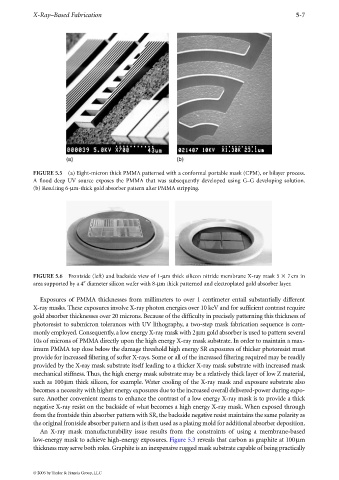
FIGURE 5.6 Frontside (left) and backside view of 1-µm thick silicon nitride membrane X-ray mask 5 7cm in
area supported by a 4 diameter silicon wafer with 8-µm thick patterned and electroplated gold absorber layer.
Exposures of PMMA thicknesses from millimeters to over 1 centimeter entail substantially different
X-ray masks. These exposures involve X-ray photon energies over 10 keV and for sufficient contrast require
gold absorber thicknesses over 20 microns. Because of the difficulty in precisely patterning this thickness of
photoresist to submicron tolerances with UV lithography, a two-step mask fabrication sequence is com-
monly employed. Consequently, a low energy X-ray mask with 2µm gold absorber is used to pattern several
10s of microns of PMMA directly upon the high energy X-ray mask substrate. In order to maintain a max-
imum PMMA top dose below the damage threshold high energy SR exposures of thicker photoresist must
provide for increased filtering of softer X-rays. Some or all of the increased filtering required may be readily
provided by the X-ray mask substrate itself leading to a thicker X-ray mask substrate with increased mask
mechanical stiffness. Thus, the high energy mask substrate may be a relatively thick layer of low Z material,
such as 100µm thick silicon, for example. Water cooling of the X-ray mask and exposure substrate also
becomes a necessity with higher energy exposures due to the increased overall delivered-power during expo-
sure. Another convenient means to enhance the contrast of a low energy X-ray mask is to provide a thick
negative X-ray resist on the backside of what becomes a high energy X-ray mask. When exposed through
from the frontside thin absorber pattern with SR, the backside negative resist maintains the same polarity as
the original frontside absorber pattern and is then used as a plating mold for additional absorber deposition.
An X-ray mask manufacturability issue results from the constraints of using a membrane-based
low-energy mask to achieve high-energy exposures. Figure 5.3 reveals that carbon as graphite at 100µm
thickness may serve both roles. Graphite is an inexpensive rugged mask substrate capable of being practically
© 2006 by Taylor & Francis Group, LLC