
Page 340 -
P. 340
5-2 MEMS: Design and Fabrication
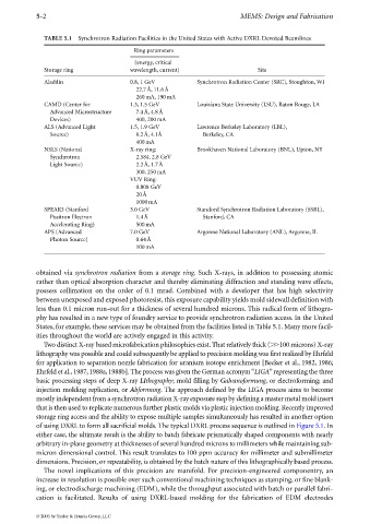
TABLE 5.1 Synchrotron Radiation Facilities in the United States with Active DXRL Devoted Beamlines
Ring parameters
(energy, critical
Storage ring wavelength, current) Site
Aladdin 0.8, 1 GeV Synchrotron Radiation Center (SRC), Stoughton, WI
22.7 Å, 11.6Å
260mA, 190mA
CAMD (Center for 1.3, 1.5 GeV Louisiana State University (LSU), Baton Rouge, LA
Advanced Microstructure 7.4Å, 4.8Å
Devices) 400, 200 mA
ALS (Advanced Light 1.5, 1.9 GeV Lawrence Berkeley Laboratory (LBL),
Source) 8.2Å, 4.1Å Berkeley, CA
400mA
NSLS (National X-ray ring: Brookhaven National Laboratory (BNL), Upton, NY
Synchrotron 2.584, 2.8 GeV
Light Source) 2.2Å, 1.7Å
300, 250mA
VUV Ring:
0.808 GeV
20Å
1000mA
SPEAR3 (Stanford 3.0 GeV Standord Synchrotron Radiation Laboratory (SSRL),
Positron Electron 1.4Å Stanford, CA
Accelerating Ring) 500mA
APS (Advanced 7.0 GeV Argonne National Laboratory (ANL), Argonne, IL
Photon Source) 0.64Å
100mA
obtained via synchrotron radiation from a storage ring. Such X-rays, in addition to possessing atomic
rather than optical absorption character and thereby eliminating diffraction and standing wave effects,
possess collimation on the order of 0.1 mrad. Combined with a developer that has high selectivity
between unexposed and exposed photoresist, this exposure capability yields mold sidewall definition with
less than 0.1 micron run-out for a thickness of several hundred microns. This radical form of lithogra-
phy has resulted in a new type of foundry service to provide synchrotron radiation access. In the United
States, for example, these services may be obtained from the facilities listed in Table 5.1. Many more facil-
ities throughout the world are actively engaged in this activity.
Two distinct X-ray based microfabrication philosophies exist. That relatively thick ( 100 microns) X-ray
lithography was possible and could subsequently be applied to precision molding was first realized by Ehrfeld
for application to separation nozzle fabrication for uranium isotope enrichment [Becker et al., 1982, 1986;
Ehrfeld et al., 1987, 1988a, 1988b]. The process was given the German acronym “LIGA”representing the three
basic processing steps of deep X-ray LIthography; mold filling by Galvanoformung, or electroforming; and
injection molding replication, or Abformung. The approach defined by the LIGA process aims to become
mostly independent from a synchrotron radiation X-ray exposure step by defining a master metal mold insert
that is then used to replicate numerous further plastic molds via plastic injection molding.Recently improved
storage ring access and the ability to expose multiple samples simultaneously has resulted in another option
of using DXRL to form all sacrificial molds. The typical DXRL process sequence is outlined in Figure 5.1.In
either case, the ultimate result is the ability to batch fabricate prismatically shaped components with nearly
arbitrary in-plane geometry at thicknesses of several hundred microns to millimeters while maintaining sub-
micron dimensional control. This result translates to 100 ppm accuracy for millimeter and submillimeter
dimensions. Precision, or repeatability, is obtained by the batch nature of this lithographically based process.
The novel implications of this precision are manifold. For precision-engineered componentry, an
increase in resolution is possible over such conventional machining techniques as stamping, or fine blank-
ing, or electrodischarge machining (EDM), while the throughput associated with batch or parallel fabri-
cation is facilitated. Results of using DXRL-based molding for the fabrication of EDM electrodes
© 2006 by Taylor & Francis Group, LLC