
Page 344 -
P. 344
5-6 MEMS: Design and Fabrication
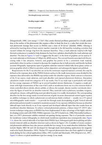
TABLE 5.3 Frequently Used Synchrotron Radiation Formulas
12398.5
Wavelength/energy conversion λ(Å)
hv(eV)
3.336E(GeV)
Bending magnet radius ρ(m) ≅
B(T)
18.64
Critical wavelength λ (Å) ≅
C B(T)E (GeV)
2
h 4.136(10) 15 eVs, ν frequency, E energy of circulating
charge particle, B bending magnet field
[Margaritondo, 1988]. Low energy ( 2keV) flux creates thermal problems generated by a locally peaked
dose at the surface of the photoresist; this requires a filter to limit the dose to a value that avoids the even-
3
tual photoresist damage that occurs in PMMA near a dose of 20 kJ/cm [Ehrfeld, 1988b]. Filtering is
achieved by inserting slices of lower atomic number materials in the SR beamline including a window that
vacuum isolates the storage ring from the exposure beamline. Thus, a mask substrate material with high
thermal conductance is needed to help dissipate the heat from radiation absorbed by the mask substrate and
absorber. The data in Figures 5.3 and 5.4 suggest that Be and C in the form of graphite can be used as X-
ray mask substrates at thicknesses of 100µm for all SR sources. The cost and hazards associated with Be pro-
cessing make it less attractive, however, and graphite has proven to be a convenient mask material,
particularly when its surface is treated to decrease the roughness due to bulk porosity and thereby facilitate
accurate lithography. Appropriate types of graphite substrate material include fully dense glassy carbon or
porous graphite which is filled via pyrolytic carbon deposition and subsequently lapped and polished.
Requirements for the X-ray absorber are set by the minimum required exposure contrast; this may be
defined as the exposure dose at the PMMA bottom surface in the mask transmission areas divided by the
exposure dose delivered to the PMMA top surface under the absorber regions. Mask contrast is a function
of the X-ray source, mask substrate, and mask absorber and exposed photoresist thickness. Absorption
calculation results reveal two categories of X-ray masks. One X-ray mask type is particularly well suited
for low energy exposures of PMMA up to several hundred micron thicknesses. It requires a mask sub-
strate with high transmission of flux near 4 keV, such as membranes from one to a few microns thick of
strain controlled silicon nitride, silicon carbide, or silicon, for example. Atomic number and density deter-
mine the figure of merit for an absorber material. Thus, materials such as platinum, tantalum, tungsten,
and gold are chosen, with gold being most prevalent because it is readily electroplated. The corresponding
absorber for the low energy mask is several microns of gold. Accurate dimensional control again requires
an additive technique in which a photoresist several microns thick is defined — usually via a UV optical
microlithographic mask transfer — to provide for through mask electroplating of gold. Vertical sidewall
photoresist pattern transfer is essential to maintain accurate X-ray exposure definition because an absorber
sidewall taper leads directly to an X-ray exposed and developed sidewall taper that also results from an
insufficient absorber thickness. To achieve vertical photoresist patterns, a bilayer deep UV (DUV) pho-
toresist technique using spun-on PMMA has been implemented. It takes advantage of the highly selective
developing system used with DXRL PMMA exposures [Lin,1975; Guckel et al.,1990].Poly(methyl methacry-
late), as a DUV photoresist exhibits minimal out-gassing during exposure. This is of particular concern
for membrane contact lithography, in which mask-membrane separation may consequently arise. Figure
5.5a. shows the vertical sidewalls of an 8µm thick PMMA layer. Subsequent gold electroplating and pho-
toresist removal yields an absorber structure such as shown in Figure 5.5b. A number of recent commer-
cial photoresist additions have also proven suitable for low energy X-ray mask absorber definition. These
include Shipley SJR5740 and 220 developed for through-mask electroplating applications for magnetic
read/write heads [Romankiw, 1995]. Thicker UV-exposed photoresists have also been applied to through
mask plating for less critical applications [Allen, 1993; Loechel and Maciossek, 1995; Despont et al., 1997].
Figure 5.6 shows a typical membrane-type low-energy X-ray mask.
© 2006 by Taylor & Francis Group, LLC