
Page 346 -
P. 346
5-8 MEMS: Design and Fabrication
used for low- and high-energy DXRL exposures; it has good thermal conductivity, and it avoids the haz-
ards and expense of beryllium and other low Z compounds and their associated processing. A carbon
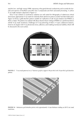
X-ray mask example is depicted in Figure 5.7.
Since X-rays emitted in synchrotron radiation are well suited for lithography of submicron critical
dimensions, appropriate X-ray masks for relatively thick submicron pattern transfer have been fabricated.
Figure 5.8 shows a gold absorber pattern suitable for replication of sub–0.2 µm features into PMMA as
thick as 10µm. The pattern was realized with direct electron beam writing of PMMA on a preformed silicon
nitride X-ray mask membrane. Challenges in X-ray patterning of thick ( 1µm) submicron features,
however, lie largely with X-ray photoresist stress, adhesion, and resulting mechanical stability, which will
be discussed in the next section.
FIGURE 5.7 X-ray mask patterned on a 3 diameter graphite support 100-µm thick with 20-µm thick gold absorber
pattern.
FIGURE 5.8 Submicron gold absorber pattern with approximately 1.0-µm thickness residing on SiN X-ray mask
membrane.
© 2006 by Taylor & Francis Group, LLC