
Page 114 - Make Your Own PCBs with EAGLE from Schematic Designs to Finished Boards
P. 114
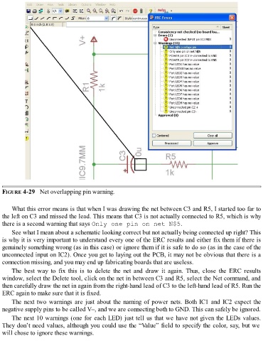
FIGURE 4-29   Net overlapping pin warning.


      What this error means is that when I was drawing the net between C3 and R5, I started too far to
  the left on C3 and missed the lead. This means that C3 is not actually connected to R5, which is why
  there is a second warning that says Only one pin on net N$5.

      See what I mean about a schematic looking correct but not actually being connected up right? This
  is why it is very important to understand every one of the ERC results and either fix them if there is
  genuinely something wrong (as in this case) or ignore them if it is safe to do so (as in the case of the
  unconnected input on IC2). Once you get to laying out the PCB, it may not be obvious that there is a
  connection missing, and you may end up fabricating boards that are useless.

      The  best  way  to  fix  this  is  to  delete  the  net  and  draw  it  again.  Thus,  close  the  ERC  results
  window, select the Delete tool, click on the net in between C3 and R5, select the Net command, and
  then carefully draw the net in again from the right-hand lead of C3 to the left-hand lead of R5. Run the
  ERC again to make sure that it is fixed.

      The next two warnings are just about the naming of power nets. Both IC1 and IC2 expect the
  negative supply pins to be called V–, and we are connecting both to GND. This can safely be ignored.

      The next 10 warnings (one for each LED) just tell us that we have not given the LEDs values.
  They don’t need values, although you could use the “Value” field to specify the color, say, but we
  will chose to ignore these warnings.