
Page 112 - Mechanical Engineers Reference Book
P. 112
Analogue and digital electronics theory 2/53
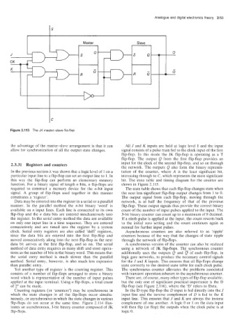
Figure 2.113 ‘The JK master-slave flip-flop
the advantage of the master-slave arrangement is that it can All J and K inputs are held at logic level 1 and the input
allow for synchronization of all the output state changes. signal consists of a pulse train fed to the clock input of the first
flip-flop. In this mode the JK flip-flop is operating as a T
flip-flop. The output Q from the first flip-flop provides an
2.3.31 Registers and counters input for the clock of the second flip-flop, and so on through
the network. The outputs Q also form the binary represen-
In the previous section it was shown that a logic level of 1 on a tation of the counter, where A is the least significant bit,
particular input line to a flip-flop can set an output line to 1. In increasing through to C, which represents the most significant
this way the flip-flop can perform an elementary memory bit. The state table and timing diagram for the counter are
function. For a binary signal of length n bits, n flip-flops are shown in Figure 2.115.
required to construct a memory device for the n-bit input The state table shows that each flip-flop changes state when
signal. A group of flip-flops used together in this manner the next less significant flip-flop output changes from 1 to 0.
constitutes a ‘register’. The output signal from each flip-flop, moving through the
Data may be entered into the register in a serial or a parallel network, is at half the frequency of that of the previous
manner. In the parallel method the n-bit binary ‘word’ is flip-flop. These output signals thus provide the correct binary
availabde on n input lines. Each line is connected to its own count of the number of input pulses applied to the input. The
flip-flop and the n data bits are entered simultaneously into 3-bit binary counter can count up to a maximum of 8 decimal.
the register. In the serial entry method the data are available If a ninth pulse is applied at the input, the count reverts back
on only one input line in a time sequence. They are entered to the initial zero setting and the count continues again as
consecutively and are timed into the register by a system normal for further input pulses.
clock. Serial entry registers are also called ’shift’ registers, Asynchronous counters are also referred to as ’ripple’
since the data bits are entered into the first flip-flop and counters because of the way that the changes of state ripple
moved consecutively along into the next flip-flop as the next through the network of flip-flops.
data bit arrives at the first flip-flop, and so on. The serial A synchronous version of the counter can also be realized
method of data entry requires as many shift and store opera- using a network of JK flip-flops. Thesynchronous counter
tions as the number of bits in the binary word. This means that additionally uses the outputs Q and Q of each flip-flop, in
the serial entry method is much slower than the parallel logic gate networks, to produce the necessary control signals
method. Serial entry, however, is also much less expensive for the J and K inputs. This ensures that a11 flip-flops change
than parallel. entry. state correctly to the desired state table for each clock pulse.
Yet another type of register Is the counting register. This The synchronous counter alleviates the problems associated
consists of a number of flip-flops arranged to store a binary with transient operation inherent in the asynchronous counter.
word which is representative of i.he number of input pulses There are, of course, many other types of flip-flop available,
applied at the input terminal. Using n flip-flops, a total count but the only one of significant practical importance is the D
of 2” can be made. flip-flop (see Figure 2.116), where the ‘D’ refers to Data.
Counting registers (or ‘counters’) may be synchronous in In the D-type flip-flop the D input is fed directly into the J
which the state changes in all the flip-flops occur simulta- input line and the inverse complement of D is fed to the K
neousby, or asynchronous in which the state changes in various input line. This ensures that J and K are always the inverse
flip-flops do not occur at the same time. Figure 2.114 illus- complement of one another. A logic 0 or 1 on the data input
trates an asynchronous, 3-bit binary counter composed of JK will then flip (or flop) the outputs when the clock pulse is at
flip-flops. logic 0.