
Page 110 - Mechanical Engineers Reference Book
P. 110
Analogue and digital electronics theory 2/51
2=F
-
CD \“” 00 01 11 10 5
00
-
E
~
F =A+ =A. F=A+B=A +5
B
01
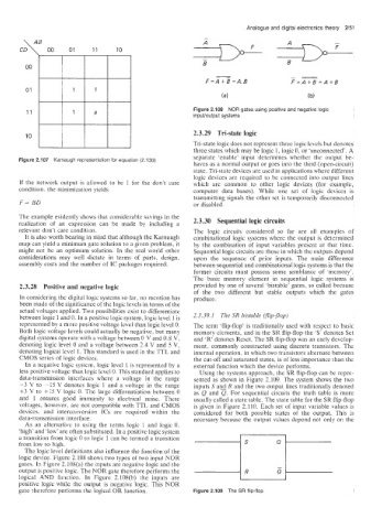
Figure 2.108 NOR gates using positive and negative logic
11 inpuffoutput systems
2.3.29 Tri-state logic
10
Tri-state logic does not represent three logic levels but denotes
three states which may be logic 1, logic 0. or ‘unconnected’. A
separate ‘enable’ input determines whether the output be-
Figure 2.107 Karnaugh representation for equation (2.130)
haves as a normal output or goes into the third (open-circuit)
state. Tri-state devices are used in applications where different
logic devices are required to be connected into output lines
If the network output is aliowed to be 1 for the don’t care which are common to other logic devices (for example,
condition. the minimization yields computer data buses). While one set of logic devices is
transmitting signals the other set is temporarily disconnected
F= BD or disabled.
The example evidently shows that considerable savings in the
realizati’on of an expression can be made by including a 2.3.30 Sequential logic circuits
relevant don’t care condition. The logic circuits considered so far are all examples of
It is al!so worth bearing in mind that although the Karnaugh combinational logic systems where the output is determined
map can yield a minimum gate solution to a given problem, it by the combination of input variables present at that time.
might not be an optimum solution. In the real world other Sequential logic circuits are those in which the outputs depend
considerations may well dictate in terms of parts, design, upon the sequence of prior inputs. The main difference
assembly costs and the number of IC packages required. between sequential and combinational logic systems is that the
former circuits must possess some semblance of ‘memory’.
The basic memory element in sequential logic systems is
2.3.28 Positive and negative logic provided by one of several ‘bistable’ gates, so called because
of the two different but stable outputs which the gates
In considering the digital logic systems so far, no mention has produce.
been made of the significance of the logic ievels in terms of the
actual voltages applied. Two possibilities exist to differentiate
between logic 1 and 0. In a positive logic system, logic level 1 is 2.3.30.1 The SR bistable (flip-flop)
represented by a more positive voltage level than logic level 0. The term ‘flip-flop’ is traditionally used with respect to basic
Both logic voltage levels could actually be negative, but many memory elements, and in the SR flip-flop the ‘S’ denotes Set
digital systems operate with a voltage between 0 V and 0.8 V, and ‘R’ denotes Reset. The SR flip-flop was an early develop-
denoting logic level 0 and a voltage between 2.4 V and 5 V, ment, commonly constructed using discrete transistors. The
denoting logical level 1. This standard is used in the TTL and internal operation, in which two transistors alternate between
CMOS series of logic devices. the cut-off and saturated states, is of less importance than the
In a negative logic system, logic level 1 is represented by a external function which the device performs.
less positive voltage than logic level 0. This standard applies to Using the systems approach, the SR flip-flop can be repre-
data-transmission interfaces where a voltage in the range sented as shown in Figure 2.109. The system shows the two
-3 V to -15 V denotes logic 1 and a voltage in the range inputs S and R and the two output lines traditionally denoted
+3 V to +15 W logic 0. The large differentiation between 0 as Q and Q. For sequential circuits the truth table is more
and 1 (ensures good immunity to electrical noise. These usually called a state table. The state table for the SR flip-flop
voltages, however, are not compatible with TTL and CMOS is given in Figure 2.110. Each set of input variable values is
devices. and interconversion ICs are required within the considered for both possible slates of the output. This is
data-trainsmission interface. necessary because the output values depend not only or, the
As an alternative to using the terms logic 1 and logic 0.
‘high’ anid ‘low’ are often substituted. In a positive logic system
a transition from logic 0 to logic P ]can be termed a transition
from low to high.
The logic level definitions also influence the function of the
logic device. Figure 2.108 shows two types of two input NOR
gates. In Figure 2.108(a) the inputs are negative logic and the
output is positive logic. The NOR gate therefore performs the
logical .4ND function. In Figure 2.108(b) the inputs are
positive logic while the output is negative logic. This NOR
gate therefore performs the logical OR function. Figure 2.109 The SR flip-flop