Page 211 -
P. 211

5.4 Future Applications  201
                                  Table 5.6. Medium configuration of aperture-type super-RENS disk
                             layer          material  thickness (nm)phase     optical constant
                                                                              n     k
                             substrate      PC       0.6 × 10 6    –          1.56  0
                             protective layer  SiN   170           –          2.35  0
                             mask layer     Sb       15            crystal    3.52  5.48
                                                                   amorphous  4.21  3.2
                             protective layer  SiN   30            –          2.35  0
                             recording layer  GeSbTe  15           crystal    3.97  4.41
                                                                   amorphous  4.29  2.09
                             protective layer  SiN   20            –          2.35  0


                                            Mark writing  Super-RENS Readout #2
                                          P = 3.0 -9.0 mW     P = 6.0 mW
                                           w
                                                               r
                                            v = 1.9 m s -1   V = 3.9 m s -1
                                                    Readout #1         Readout #3
                                                    P  = 1.5 mW       P  = 1.5 mW
                                                                       r
                                                     r
                                                    v = 1.9 m s -1    v = 1.9 m s -1
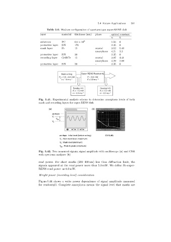
                            Fig. 5.41. Experimental analysis scheme to determine amorphous levels of both
                            mask and recording layers for super-RENS disk

                                   (a)                           (b)
                                     as-depo
                                     V 1
                                        V pp
                                     V
                                      2


                                          as-depo: Initial level (before writing)  CNR(dB)
                                          V  : Non-mark level (maximum)
                                           1
                                          V  : Mark level (minimum)
                                           2
                                          V : Peak to peak (amplitude)
                                           pp
                            Fig. 5.42. Two measured signals; signal amplitude with oscilloscope (a)and CNR
                            with spectrum analyzer (b)

                            read power. For short marks (200–400 nm) less than diffraction limit, the
                            signals appeared at the read power more than 5.0 mW. We define Sb-super-
                            RENS read power as 6.0 mW.

                            Wright power (recording level) consideration
                            Figure 5.44 shows a write power dependence of signal amplitude measured
                            for readout#1. Complete amorphous means the signal level that marks are
   206   207   208   209   210   211   212   213   214   215   216