
Page 68 -
P. 68
2.4 Applications 57
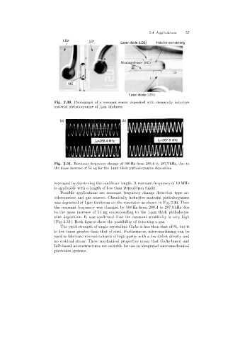
LD2 LD1 Laser diode (LD2) Hole for wet-etching
Microcantilever (MC)
MC
Laser diode (LD1)
Fig. 2.30. Photograph of a resonant sensor deposited with chemically inductive
material phthalocyanine of 1 µm thickness
(a) (b)
f =288.4 kHz f 0 =287.9 kHz
0
Fig. 2.31. Resonant frequency change of 500 Hz from 288.4 to 287.9 kHz, due to
the mass increase of 54 ng for the 1-µm thick phthalocyanine deposition
increased by shorteningthe cantilever length. A resonant frequency of 10 MHz
is applicable with a length of less than 20 µm(3 µmthick).
Possible applications are resonant frequency change detection type ac-
celerometers and gas sensors. Chemically inductive material phthalocyanine
was deposited of 1 µm thickness on the resonator as shown in Fig. 2.30. Then
the resonant frequency was changed by 500 Hz from 288.4 to 287.9 kHz due
to the mass increase of 54 ngcorrespondingto the 1-µm thick phthalocya-
nine deposition. It was confirmed that the resonant sensitivity is very high
(Fig. 2.31). Both figures show the possibility of detecting a gas.
The yield strength of single crystalline GaAs is less than that of Si, but it
is five times greater than that of steel. Furthermore, micromachining can be
used to fabricate microstructures of high purity with a low defect density and
no residual stress. These mechanical properties mean that GaAs-based and
InP-based microstructures are suitable for use in integrated micromechanical
photonics systems.