
Page 70 -
P. 70
2.4 Applications 59
An LD monolithically integrated with a PD is mounted junction-up on a
slider. Light reflects from the medium back into the active region of the LD.
Head-medium spacing h (between the LD facet and the GeSbTe recording
medium) is approximately 2 µm: the sum of the slider flyingheight h 0 ,LD–
PD attachment error h 1 , and the protective layer thickness h 2 .
Head Structure
A monolithically integrated LD–PD chip with a wavelength of 1.3 µmwas
shown in Fig. 1.33. The LD is isolated from the PD by reactive ion beam
etching(RIBE). The space between LD and PD is about 5 µm and the monitor
current sensitivity is 0.1 mA/mW. The 1.2-µm-wide taper-ridged waveguide
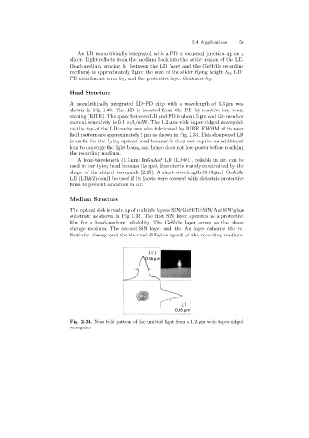
on the top of the LD cavity was also fabricated by RIBE. FWHM of its near
field pattern are approximately 1 µm as shown in Fig. 2.34. This sharpened LD
is useful for the flyingoptical head because it does not require an additional
lens to converge the light beam, and hence does not lose power before reaching
the recordingmedium.
A long-wavelength (1.3 µm) InGaAsP LD (LD#1), reliable in air, can be
used in our flyinghead because its spot diameter is mainly constrained by the
shape of the ridged waveguide [2.25]. A short-wavelength (0.83 µm) GaAlAs
LD (LD#2) could be used if its facets were covered with dielectric protective
films to prevent oxidation in air.
Medium Structure
The optical disk is made up of multiple layers: SiN/GeSbTe/SiN/Au/SiN/glass
substrate as shown in Fig. 1.32. The first SiN layer operates as a protective
film for a head-medium reliability. The GeSbTe layer serves as the phase
change medium. The second SiN layer and the Au layer enhance the re-
flectivity change and the thermal diffusion speed of the recording medium.
(//)
0.85 mm
(T)
0.65 mm
Fig. 2.34. Near field pattern of the emitted light from a 1.2-µm wide taper-ridged
waveguide