
Page 113 - A Practical Guide from Design Planning to Manufacturing
P. 113
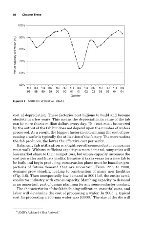
86   Chapter Three


           100%


          Wafer capacity utilization (%)  80%
            90%


            70%


            60%


            50%
                1Q  3Q  1Q  3Q  1Q  3Q  1Q  3Q  1Q  3Q  1Q  3Q  1Q  3Q
                98  98  99  99  00  00  01  01  02  02  03  03  04  04
                                        Quarter
        Figure 3-6 MOS fab utilization. (ibid.)


        cost of depreciation. These factories cost billions to build and become
        obsolete in a few years. This means the depreciation in value of the fab
        can be more than a million dollars every day. This cost must be covered
        by the output of the fab but does not depend upon the number of wafers
        processed. As a result, the biggest factor in determining the cost of pro-
        cessing a wafer is typically the utilization of the factory. The more wafers
        the fab produces, the lower the effective cost per wafer.
          Balancing fab utilization is a tightrope all semiconductor companies
        must walk. Without sufficient capacity to meet demand, companies will
        lose market share to their competitors, but excess capacity increases the
        cost per wafer and hurts profits. Because it takes years for a new fab to
        be built and begin producing, construction plans must be based on pro-
        jections of future demand that are uncertain. From 1999 to 2000,
        demand grew steadily, leading to construction of many new facilities
        (Fig. 3-6). Then unexpectedly low demand in 2001 left the entire semi-
        conductor industry with excess capacity. Matching capacity to demand
        is an important part of design planning for any semiconductor product.
          The characteristics of the fab including utilization, material costs, and
        labor will determine the cost of processing a wafer. In 2003, a typical
                                                   5
        cost for processing a 200-mm wafer was $3000. The size of the die will


          5
          “AMD’s Athlon 64 Has Arrived.”