Page 115 - A Practical Guide from Design Planning to Manufacturing
P. 115
88 Chapter Three
Unfortunately not all the die produced will function properly. In fact,
although it is something each factory strives for, in the long run 100 percent
yield will not give the highest profits. Reducing the on-die dimensions
allows more die per wafer and higher frequencies that can be sold at
higher prices. As a result, the best profits are achieved when the process
is always pushed to the point where at least some of the die fail. The
density of defects and complexity of the manufacturing process deter-
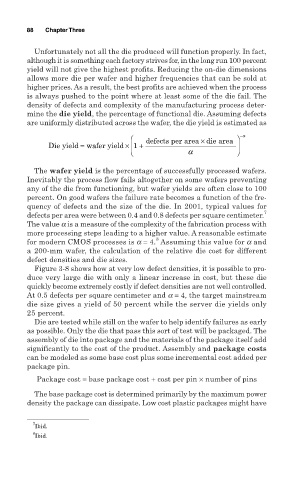
mine the die yield, the percentage of functional die. Assuming defects
are uniformly distributed across the wafer, the die yield is estimated as
defects per area diee area − α
×
Die yield = wafer yield × 1 +
α
The wafer yield is the percentage of successfully processed wafers.
Inevitably the process flow fails altogether on some wafers preventing
any of the die from functioning, but wafer yields are often close to 100
percent. On good wafers the failure rate becomes a function of the fre-
quency of defects and the size of the die. In 2001, typical values for
7
defects per area were between 0.4 and 0.8 defects per square centimeter.
The value a is a measure of the complexity of the fabrication process with
more processing steps leading to a higher value. A reasonable estimate
8
for modern CMOS processes is a = 4. Assuming this value for a and
a 200-mm wafer, the calculation of the relative die cost for different
defect densities and die sizes.
Figure 3-8 shows how at very low defect densities, it is possible to pro-
duce very large die with only a linear increase in cost, but these die
quickly become extremely costly if defect densities are not well controlled.
At 0.5 defects per square centimeter and a = 4, the target mainstream
die size gives a yield of 50 percent while the server die yields only
25 percent.
Die are tested while still on the wafer to help identify failures as early
as possible. Only the die that pass this sort of test will be packaged. The
assembly of die into package and the materials of the package itself add
significantly to the cost of the product. Assembly and package costs
can be modeled as some base cost plus some incremental cost added per
package pin.
Package cost = base package cost + cost per pin × number of pins
The base package cost is determined primarily by the maximum power
density the package can dissipate. Low cost plastic packages might have
7
Ibid.
8
Ibid.

