
Page 269 - A Practical Guide from Design Planning to Manufacturing
P. 269
Layout 241
Length
N+
diffusion Length
Poly
gate
Width
Poly
Width S S S S Source e e e Drain
gate
Source Drain
N+
P-well P-well Diffusion
Transistor cross section Transistor layout
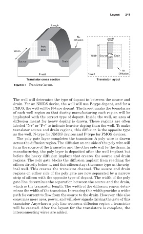
Figure 8-1 Transistor layout.
The well will determine the type of dopant in between the source and
drain. For an NMOS device, the well will use P-type dopant, and for a
PMOS, the well will be N-type dopant. The layout marks the boundaries
of each well region so that during manufacturing each region will be
implanted with the correct type of dopant. Inside the well, an area of
diffusion meant for heavy doping is drawn. These regions are often
labeled “N+” or “P+” to indicate heavier doping than the well. To make
transistor source and drain regions, this diffusion is the opposite type
as the well, N-type for NMOS devices and P-type for PMOS devices.
The poly gate layer completes the transistor. A poly wire is drawn
across the diffusion region. The diffusion on one side of the poly wire will
form the source of the transistor and the other side will be the drain. In
manufacturing, the poly layer is deposited after the well implant but
before the heavy diffusion implant that creates the source and drain
regions. The poly gate blocks the diffusion implant from reaching the
silicon directly below it, and this silicon stays the same type as the orig-
inal well. This creates the transistor channel. The source and drain
regions on either side of the poly gate are now separated by a narrow
strip of silicon with the opposite type of dopant. The width of the poly
gate line determines the separation between the source and the drain,
which is the transistor length. The width of the diffusion region deter-
mines the width of the transistor. Increasing this width provides a wider
path for current to flow from the source to the drain. However, this also
consumes more area, power, and will slow signals driving the gate of this
transistor. Anywhere a poly line crosses a diffusion region a transistor
will be created. After the layout for the transistors is complete, the
interconnecting wires are added.