
Page 274 - A Practical Guide from Design Planning to Manufacturing
P. 274
Layout 245
The PMOS device uses P-type source and drain in an N-well with an
N-type well tap. The NMOS device is the exact opposite with N-type
source and drain in a P-well with a P-type well tap.
In step 2, the connections to the supply voltage (V dd ) and the ground
voltage (V ss ) are made. The mask designer chooses which side of the tran-
sistor to use as the source terminal and places as many contacts as there
is room for along that side. Also, one contact is placed on each well tap.
Two metal 1 wires are drawn to bring the needed voltage to the contacts.
Presumably these metal 1 wires will be connected to other wires at a
higher level when the inverter layout is used. Step 3 connects the inverter
input and output. The input is drawn in metal 1 and goes through a con-
tact to drive both poly gates. The output is also drawn in metal 1 and uses
multiple contacts to connect to the drain diffusion of each transistor.
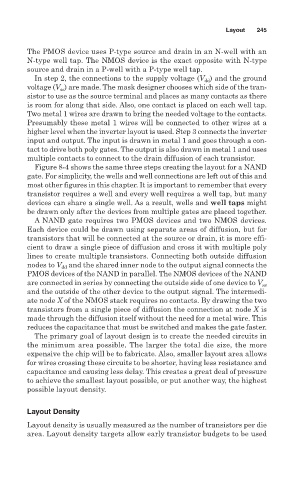
Figure 8-4 shows the same three steps creating the layout for a NAND
gate. For simplicity, the wells and well connections are left out of this and
most other figures in this chapter. It is important to remember that every
transistor requires a well and every well requires a well tap, but many
devices can share a single well. As a result, wells and well taps might
be drawn only after the devices from multiple gates are placed together.
A NAND gate requires two PMOS devices and two NMOS devices.
Each device could be drawn using separate areas of diffusion, but for
transistors that will be connected at the source or drain, it is more effi-
cient to draw a single piece of diffusion and cross it with multiple poly
lines to create multiple transistors. Connecting both outside diffusion
nodes to V and the shared inner node to the output signal connects the
dd
PMOS devices of the NAND in parallel. The NMOS devices of the NAND
are connected in series by connecting the outside side of one device to V ss
and the outside of the other device to the output signal. The intermedi-
ate node X of the NMOS stack requires no contacts. By drawing the two
transistors from a single piece of diffusion the connection at node X is
made through the diffusion itself without the need for a metal wire. This
reduces the capacitance that must be switched and makes the gate faster.
The primary goal of layout design is to create the needed circuits in
the minimum area possible. The larger the total die size, the more
expensive the chip will be to fabricate. Also, smaller layout area allows
for wires crossing these circuits to be shorter, having less resistance and
capacitance and causing less delay. This creates a great deal of pressure
to achieve the smallest layout possible, or put another way, the highest
possible layout density.
Layout Density
Layout density is usually measured as the number of transistors per die
area. Layout density targets allow early transistor budgets to be used