
Page 278 - A Practical Guide from Design Planning to Manufacturing
P. 278
248 Chapter Eight
D2 C3
P3 D4 3l
W W W 16l
p p
M2 C1 M2 3l
44l C4 1l
M1 C1 2l
C4 C4 1l
M2 3l
M3
C2 2
D1
W W W 12l
n n
D4 D4 3l
P1
D4 D1 D2 C4 C1 C3 P1 C3 C1 C4 D4
3l 4l 2l 1l 2l 2l 2l 2l 2l 1l 3l
24l
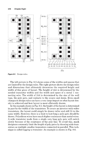
Figure 8-5 Design rules.
The left picture in Fig. 8-5 shows some of the widths and spaces that
are limited by the design rules. The right picture shows the design rules
and dimensions that ultimately determine the required height and
width of this piece of layout. The height of 44l is determined by the
needed transistor widths and the width and space of a metal 1 con-
necting wire. The width of 24l is determined by the size of the well
taps, the poly gate, and contacts to the source and drain. Even small
changes in design rules can have a very large impact on what layout den-
sity is achieved and how layout is most efficiently drawn.
In the example shown in Fig. 8-5, the height of the layout is determined
in part by the width of the transistors. To create an inverter with wider
transistors, the layout could simply be drawn taller and still fit in the
same width. However, there is a limit to how long a poly gate should be
drawn. Polysilicon wires have much higher resistance than metal wires.
A wide transistor made from a single very long poly gate will switch
slowly because of the resistance of the poly line. To avoid this, mask
designers commonly limit the length of poly gates by drawing wide tran-
sistors as multiple smaller transistors connected in parallel. This tech-
nique is called legging a transistor. An example is shown in Fig. 8-6.