
Page 279 - A Practical Guide from Design Planning to Manufacturing
P. 279
Layout 249
Single leg inverter
Double leg inverter
V V V dd
V V V dd
W W W = 24
p p
V V V dd V V V dd
In Out W W W = 24
p p
W W W = 16 W W W = 12
n n
p p
V V V ss
In Out In Out
P+
N+
W W W = 8
Poly n n
W W W = 16
n n
Contact V V V ss V V V ss
M1
V V V ss
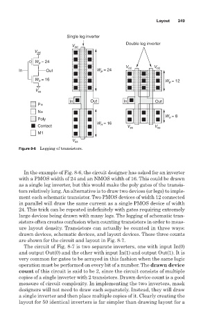
Figure 8-6 Legging of transistors.
In the example of Fig. 8-6, the circuit designer has asked for an inverter
with a PMOS width of 24 and an NMOS width of 16. This could be drawn
as a single leg inverter, but this would make the poly gates of the transis-
tors relatively long. An alternative is to draw two devices (or legs) to imple-
ment each schematic transistor. Two PMOS devices of width 12 connected
in parallel will draw the same current as a single PMOS device of width
24. This trick can be repeated indefinitely with gates requiring extremely
large devices being drawn with many legs. The legging of schematic tran-
sistors often creates confusion when counting transistors in order to meas-
ure layout density. Transistors can actually be counted in three ways:
drawn devices, schematic devices, and layout devices. These three counts
are shown for the circuit and layout in Fig. 8-7.
The circuit of Fig. 8-7 is two separate inverters, one with input In(0)
and output Out(0) and the other with input In(1) and output Out(1). It is
very common for gates to be arrayed in this fashion when the same logic
operation must be performed on every bit of a number. The drawn device
count of this circuit is said to be 2, since the circuit consists of multiple
copies of a single inverter with 2 transistors. Drawn device count is a good
measure of circuit complexity. In implementing the two inverters, mask
designers will not need to draw each separately. Instead, they will draw
a single inverter and then place multiple copies of it. Clearly creating the
layout for 50 identical inverters is far simpler than drawing layout for a