
Page 283 - A Practical Guide from Design Planning to Manufacturing
P. 283
Layout 253
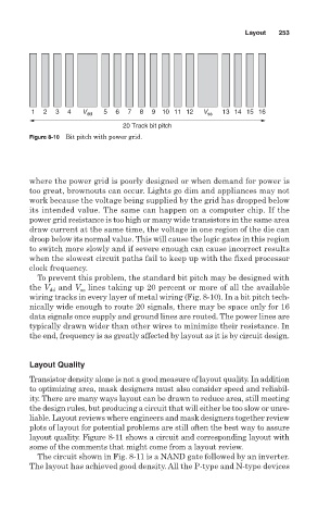
1 2 3 4 V dd 5 6 7 8 9 10 11 12 V ss 13 14 15 16
20 Track bit pitch
Figure 8-10 Bit pitch with power grid.
where the power grid is poorly designed or when demand for power is
too great, brownouts can occur. Lights go dim and appliances may not
work because the voltage being supplied by the grid has dropped below
its intended value. The same can happen on a computer chip. If the
power grid resistance is too high or many wide transistors in the same area
draw current at the same time, the voltage in one region of the die can
droop below its normal value. This will cause the logic gates in this region
to switch more slowly and if severe enough can cause incorrect results
when the slowest circuit paths fail to keep up with the fixed processor
clock frequency.
To prevent this problem, the standard bit pitch may be designed with
the V dd and V lines taking up 20 percent or more of all the available
ss
wiring tracks in every layer of metal wiring (Fig. 8-10). In a bit pitch tech-
nically wide enough to route 20 signals, there may be space only for 16
data signals once supply and ground lines are routed. The power lines are
typically drawn wider than other wires to minimize their resistance. In
the end, frequency is as greatly affected by layout as it is by circuit design.
Layout Quality
Transistor density alone is not a good measure of layout quality. In addition
to optimizing area, mask designers must also consider speed and reliabil-
ity. There are many ways layout can be drawn to reduce area, still meeting
the design rules, but producing a circuit that will either be too slow or unre-
liable. Layout reviews where engineers and mask designers together review
plots of layout for potential problems are still often the best way to assure
layout quality. Figure 8-11 shows a circuit and corresponding layout with
some of the comments that might come from a layout review.
The circuit shown in Fig. 8-11 is a NAND gate followed by an inverter.
The layout has achieved good density. All the P-type and N-type devices