
Page 285 - A Practical Guide from Design Planning to Manufacturing
P. 285
Layout 255
Good:
#1 - Bad: Inverter legs
Out# Diffusion not
Out driven in
fully strapped parallel
A V V V dd
B
1
#2 - Bad:
Output
P+ diffusion not 2 2
N+ shared
Poly A 3 Out# 2 2
Contact
3
M1 B Out
4
#4 - Bad: V V V
Unneeded ss #3 - Bad:
contacts Minimum
width field
poly
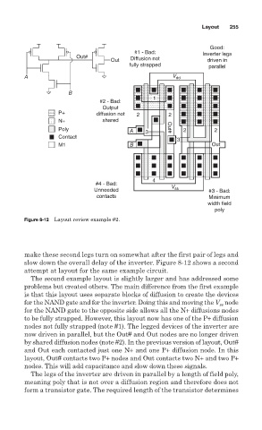
Figure 8-12 Layout review example #2.
make these second legs turn on somewhat after the first pair of legs and
slow down the overall delay of the inverter. Figure 8-12 shows a second
attempt at layout for the same example circuit.
The second example layout is slightly larger and has addressed some
problems but created others. The main difference from the first example
is that this layout uses separate blocks of diffusion to create the devices
for the NAND gate and for the inverter. Doing this and moving the V node
ss
for the NAND gate to the opposite side allows all the N+ diffusions nodes
to be fully strapped. However, this layout now has one of the P+ diffusion
nodes not fully strapped (note #1). The legged devices of the inverter are
now driven in parallel, but the Out# and Out nodes are no longer driven
by shared diffusion nodes (note #2). In the previous version of layout, Out#
and Out each contacted just one N+ and one P+ diffusion node. In this
layout, Out# contacts two P+ nodes and Out contacts two N+ and two P+
nodes. This will add capacitance and slow down these signals.
The legs of the inverter are driven in parallel by a length of field poly,
meaning poly that is not over a diffusion region and therefore does not
form a transistor gate. The required length of the transistor determines