
Page 286 - A Practical Guide from Design Planning to Manufacturing
P. 286
256 Chapter Eight
the width of gate poly, but field poly does not affect any transistor param-
eters. Because of the high resistance of poly, field poly should be drawn
at greater than minimum width where possible. In this layout, the long
lengths of minimum width field poly will add resistance and slow down
the switching of the gates (note #3). Finally, the intermediate node
between the two N-devices of the NAND gate is drawn with contacts
when this node does not need to be connected to any metal wires (note #4).
The space between the two N-devices could be reduced if these unneces-
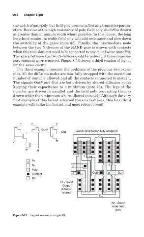
sary contacts were removed. Figure 8-13 shows a third version of layout
for the same circuit.
The third example corrects the problems of the previous two exam-
ples. All the diffusion nodes are now fully strapped with the maximum
number of contacts allowed and all the contacts connected to metal 1.
The signals Out# and Out are both driven by shared diffusion nodes
keeping their capacitance to a minimum (note #1). The legs of the
inverter are driven in parallel and the field poly connecting them is
drawn wider than minimum where allowed (note #2). Although the very
first example of this layout achieved the smallest area, this final third
example will make the fastest and most robust circuit.
Out# Good: All diffusion fully strapped
Out
V V V dd
A
B
1
P+
N+ A 1
Poly
Contact B Out# 2 Out
M1
#1 - Good:
Output
diffusion
shared
V V V ss
#2 - Good:
wide field
poly
Figure 8-13 Layout review example #3.