
Page 284 - A Practical Guide from Design Planning to Manufacturing
P. 284
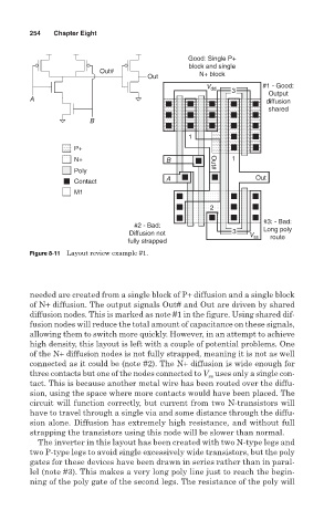
254   Chapter Eight


                                               Good: Single P+
                                               block and single
                         Out#                     N+ block
                                     Out
                                                   V V V dd  3   #1 - Good:
                                                                   Output
        A                                                         diffusion
                                                                   shared
                       B

                                               1
                   P+
                   N+                     B          Out#  1
                   Poly
                                          A                     Out
                   Contact
                   M1

                                                    2 2 2 2 2 2 2 2 2 2
                                                                 #3: - Bad:
                                  #2 - Bad:
                                 Diffusion not            3   V V V ss  Long poly
                                                                   route
                                fully strapped
        Figure 8-11 Layout review example #1.


        needed are created from a single block of P+ diffusion and a single block
        of N+ diffusion. The output signals Out# and Out are driven by shared
        diffusion nodes. This is marked as note #1 in the figure. Using shared dif-
        fusion nodes will reduce the total amount of capacitance on these signals,
        allowing them to switch more quickly. However, in an attempt to achieve
        high density, this layout is left with a couple of potential problems. One
        of the N+ diffusion nodes is not fully strapped, meaning it is not as well
        connected as it could be (note #2). The N+ diffusion is wide enough for
        three contacts but one of the nodes connected to V uses only a single con-
                                                    ss
        tact. This is because another metal wire has been routed over the diffu-
        sion, using the space where more contacts would have been placed. The
        circuit will function correctly, but current from two N-transistors will
        have to travel through a single via and some distance through the diffu-
        sion alone. Diffusion has extremely high resistance, and without full
        strapping the transistors using this node will be slower than normal.
          The inverter in this layout has been created with two N-type legs and
        two P-type legs to avoid single excessively wide transistors, but the poly
        gates for these devices have been drawn in series rather than in paral-
        lel (note #3). This makes a very long poly line just to reach the begin-
        ning of the poly gate of the second legs. The resistance of the poly will