
Page 282 - A Practical Guide from Design Planning to Manufacturing
P. 282
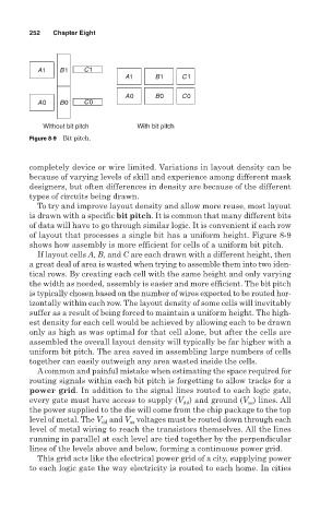
252   Chapter Eight


          A1    B1    C1
                                A1     B1     C1

                                A0     B0     C0
          A0    B0    C0

            Without bit pitch      With bit pitch
        Figure 8-9 Bit pitch.


        completely device or wire limited. Variations in layout density can be
        because of varying levels of skill and experience among different mask
        designers, but often differences in density are because of the different
        types of circuits being drawn.
          To try and improve layout density and allow more reuse, most layout
        is drawn with a specific bit pitch. It is common that many different bits
        of data will have to go through similar logic. It is convenient if each row
        of layout that processes a single bit has a uniform height. Figure 8-9
        shows how assembly is more efficient for cells of a uniform bit pitch.
          If layout cells A, B, and C are each drawn with a different height, then
        a great deal of area is wasted when trying to assemble them into two iden-
        tical rows. By creating each cell with the same height and only varying
        the width as needed, assembly is easier and more efficient. The bit pitch
        is typically chosen based on the number of wires expected to be routed hor-
        izontally within each row. The layout density of some cells will inevitably
        suffer as a result of being forced to maintain a uniform height. The high-
        est density for each cell would be achieved by allowing each to be drawn
        only as high as was optimal for that cell alone, but after the cells are
        assembled the overall layout density will typically be far higher with a
        uniform bit pitch. The area saved in assembling large numbers of cells
        together can easily outweigh any area wasted inside the cells.
          Acommon and painful mistake when estimating the space required for
        routing signals within each bit pitch is forgetting to allow tracks for a
        power grid. In addition to the signal lines routed to each logic gate,
        every gate must have access to supply (V ) and ground (V ) lines. All
                                              dd
                                                              ss
        the power supplied to the die will come from the chip package to the top
        level of metal. The V and V voltages must be routed down through each
                                 ss
                          dd
        level of metal wiring to reach the transistors themselves. All the lines
        running in parallel at each level are tied together by the perpendicular
        lines of the levels above and below, forming a continuous power grid.
          This grid acts like the electrical power grid of a city, supplying power
        to each logic gate the way electricity is routed to each home. In cities