
Page 277 - A Practical Guide from Design Planning to Manufacturing
P. 277
Layout 247
in estimating the die area required by each portion of the design, which
provides an estimate of what the total die area will ultimately be. Failure
to meet these density targets can lead to products that are more costly
or have less performance than expected. The number and size of tran-
sistors needed as well as the limits of the manufacturing process deter-
mine the layout area required by a circuit.
A wire drawn too thin may be manufactured with breaks in the wire,
preventing a good electrical connection. A pair of wires drawn too close
together may touch where they are not supposed to, creating an electri-
cal short. To prevent these problems, process engineers create layout
design rules that restrict the minimum widths and spaces of all the
layers. Additional rules set minimum overlaps or spaces between dif-
ferent layers. The goal is to create a set of rules such that any layout that
meets these guidelines can be manufactured with high yield. Table 8-1
shows an example set of design rules.
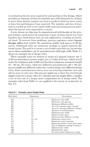
These example rules are written in terms of a generic feature size l.
A 90-nm generation process might use a l value of 45-nm, which would
make the minimum poly width and therefore minimum transistor length
2l = 90-nm. Of course, what two different manufactures call a “90-nm”
process might use different values for l and perhaps very different design
rules. Some manufacturers focus more on reducing transistor size and
others more on wire size. One process might use a short list of relatively
simple rules but a large value of l. Another process might allow a smaller
l but at the cost of a longer more complicated set of design rules. The
example rules from Table 8-1 are applied to the layout of an inverter in
Fig. 8-5.
TABLE 8-1 Example Layout Design Rules
Rule label Dimension Description
W1 4l Minimum well width
W2 2l Minimum well spacing
D1 4l Minimum diffusion width
D2 2l N+ to P+ spacing (same voltage)
D3 6l N+ to P+ spacing (different voltage)
D4 3l Diffusion to well boundary
P1 2l Minimum poly width
P2 2l Minimum poly space
P3 1l Minimum poly diffusion overlap
C1 2l × 2l Minimum contact area
C2 2l Minimum contact spacing
C3 2l Minimum contact to gate poly space
C4 1l Poly or diffusion overlap of contact
M1 3l Minimum M1 width
M2 3l Minimum M1 space
M3 1l M1 and contact minimum overlap