Page 273 - A Practical Guide from Design Planning to Manufacturing
P. 273

Out                        Out

                                                                  3
                                                                  Step
               V dd  V  V     V ss  V  V  V dd  V  V          V ss  V  V
                       In
                                                  In


                                                                  2
                                                                  Step
               V dd  V  V     V ss  V  V  V dd  V  V          V ss  V  V


                                        PMOS  P  W p  W  W  p  NMOS  Wn


                                         P+              N+
              PMOS  W p /L  W  W  W n /L  W  W  NMOS  L  P+  L  N+  1  Step

                                               N-Well          P-Well
                                   N+                     P+


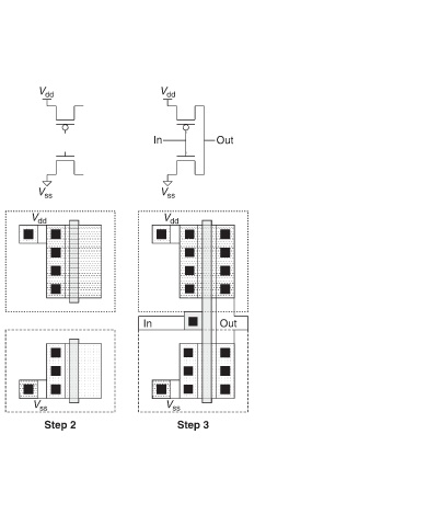
                                    Well  tap              Well  tap  Inverter layout.
                       Out

               V dd  V  V  W p /L  W  W  W n /L  W  W  V ss  V  V
                                      N-well  P-well  P+  N+  Poly  Contact  M1  Figure 8-3

                       In                                   Palate


        244
   268   269   270   271   272   273   274   275   276   277   278