
Page 271 - A Practical Guide from Design Planning to Manufacturing
P. 271
Layout 243
Vias are vertical columns of metal between levels of wires. Just like
contacts they form vertical connections, but between wires instead of
between wires and transistors. The via1 layer creates connections between
metal 1 and metal 2 wires above. A layer of insulation separates each
wiring level so that connections are made between levels only where vias
are drawn. This allows metal 2 wires to cross over metal 1 without making
contact. Later, another via1 could take the electrical signal back down to
metal 1 where a contact could then connect to the appropriate transistor.
Modern microprocessors might use seven or more layers of vias and
metal wires to make all the needed connections between hundreds of mil-
lions of transistors. Each metal layer uses one type of via to connect to the
layer below and another type to connect to the layer above. With the excep-
tion of metal 1, each metal layer typically has all the wires drawn in the
same direction. For instance, metal layers 2, 4, and 6 might contain wires
traveling east to west across the die whereas layers 3, 5, and 7 travel
north to south. Alternating layers in this fashion allow all the wires on one
level to be drawn in parallel, making the best use of area while still allow-
ing connections to be made between any two points on the die by just
using more than one layer. Adding more layers of metal interconnect may
allow more efficient connections and a smaller die, but each new layer adds
cost to the manufacturing process. Combining the layers required for tran-
sistors and those for interconnects allows any needed circuit to be drawn.
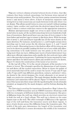
Figure 8-3 shows the construction of the layout of an inverter.
At the top left of Fig. 8-3 is the circuit schematic of the inverter to be
drawn in layout. The schematic specifies the dimensions of each transis-
tor and shows all the needed connections. Below is shown the palate of
seven materials that will be used to create the layout: P-type and N-type
wells, P-type and N-type diffusion, polysilicon, contacts, and metal 1 wires.
As drawn by the circuit designer, the circuit schematic is not meant to
imply any particular orientation. The mask designer decides where each
transistor and connection will be placed. Figure 8-3 breaks the construc-
tion of this layout into three steps with the top showing the circuit schematic
oriented, as imagined by the mask designer, and the bottom showing the
layout.
The first step is creating the transistors themselves. Step 1 shows the
layout for a PMOS transistor and an NMOS transistor. Drawing a well
with two rectangles of diffusion inside forms each transistor. One piece
of diffusion forms the well tap, which provides an electrical connection
to hold the well at a fixed voltage. The well tap is drawn as the same
dopant type as the well. The other rectangle of diffusion is the opposite
type of the well and forms the transistor source and drain regions. A
piece of poly drawn across this diffusion forms the transistor gate. The
width of the poly gate determines the length of the transistor and
the width of diffusion it crosses determines the width of the transistor.