
Page 270 - A Practical Guide from Design Planning to Manufacturing
P. 270
242 Chapter Eight
Metal 2 Via 1
Via 1
Metal 2
Contact
Contact
Metal 1
Metal1
Poly
gate Transistor layout
Contact
P-well Metal 1
Source Drain
N+ Via1
Poly Metal 2
P-well
Transistor cross section Layout key
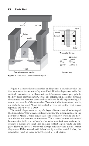
Figure 8-2 Transistor and interconnect layout.
Figure 8-2 shows the cross section and layout of a transistor with the
first two metal interconnect layers added. The first layer created is the
vertical contacts that will connect the diffusion regions or poly gate to
the first layer of interconnect. These are columns of metal that form all
the connections between wires and transistors. To aid in processing, all
contacts are made of the same size. To contact wide transistors, multi-
ple contacts are used. Above the contact layer is the first layer of wires,
typically called metal 1 (M1).
The metal 1 layer rests on top of a layer of insulation added on top of
the transistors. This prevents it from touching the silicon surface or the
poly layer. Metal 1 wires can create connections by crossing the hori-
zontal distance between two contacts. The drain of one transistor can
be connected to the gate of another by using a contact to go up from the
drain to a metal 1 wire and then another contact to go down to the poly
gate. However, metal 1 wires will always contact other metal 1 wires
they cross. If the needed path is blocked by another metal 1 wire, the
connection must be made using the next level of wiring.